The following content is an automatically extracted verbatim text
from the original manufacturer datasheet and is provided for reference purposes only.
View original datasheet text
www.DataSheet4U.com
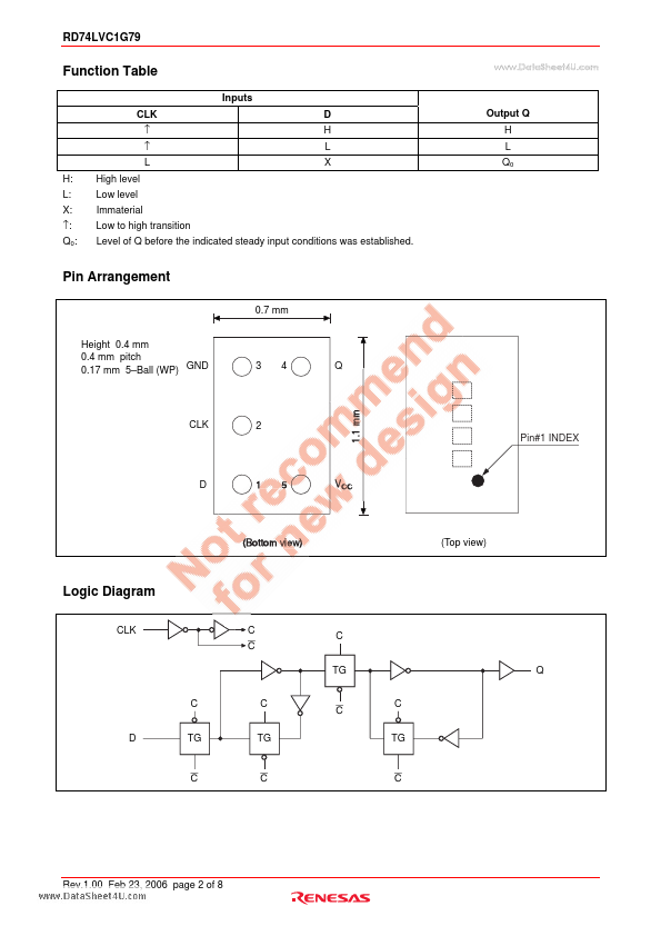
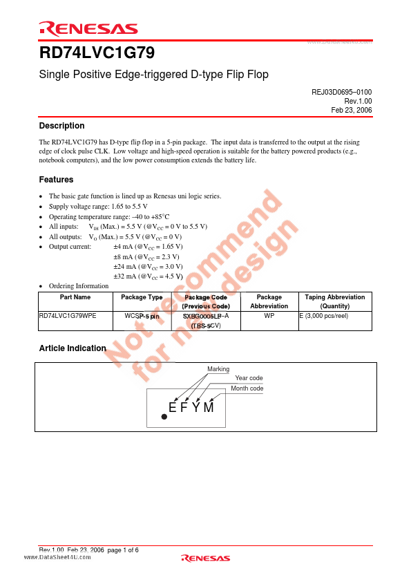
RD74LVC1G79
Single Positive Edge-triggered D-type Flip Flop
REJ03D0695–0100 Rev.1.00 Feb 23, 2006
Description
The RD74LVC1G79 has D-type flip flop in a 5-pin package. The input data is transferred to the output at the rising edge of clock pulse CLK. Low voltage and high-speed operation is suitable for the battery powered products (e.g., notebook computers), and the low power consumption extends the battery life.
Features
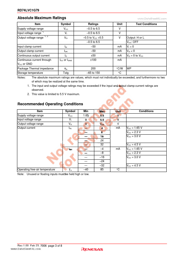
The basic gate function is lined up as Renesas uni logic series. Supply voltage range: 1.65 to 5.5 V Operating temperature range: –40 to +85°C All inputs: VIH (Max.) = 5.5 V (@VCC = 0 V to 5.5 V) All outputs: VO (Max.) = 5.5 V (@VCC = 0 V) Output current: ±4 mA (@VCC = 1.65 V) ±8 mA (@VCC = 2.3 V) ±24 mA (@VCC = 3.0 V) ±32 mA (@VCC = 4.
 RD74LVC1G79 Datasheet