Click to expand full text
www.DataSheet4U.com
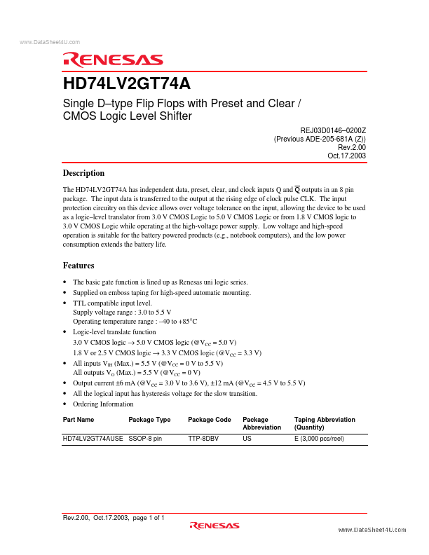
HD74LV2GT74A
Single D–type Flip Flops with Preset and Clear / CMOS Logic Level Shifter
REJ03D0146–0200Z (Previous ADE-205-681A (Z)) Rev.2.00 Oct.17.2003
Description
The HD74LV2GT74A has independent data, preset, clear, and clock inputs Q and Q outputs in an 8 pin package. The input data is transferred to the output at the rising edge of clock pulse CLK. The input protection circuitry on this device allows over voltage tolerance on the input, allowing the device to be used as a logic–level translator from 3.0 V CMOS Logic to 5.0 V CMOS Logic or from 1.8 V CMOS logic to 3.0 V CMOS Logic while operating at the high-voltage power supply. Low voltage and high-speed operation is suitable for the battery powered products (e.g.
 HD74LV2GT74A Datasheet