Datasheet Details
| Part number | HD74LV1G125A |
|---|---|
| Manufacturer | Renesas |
| File Size | 137.15 KB |
| Description | Bus Buffer Gate |
| Datasheet |
 HD74LV1G125A Datasheet HD74LV1G125A Datasheet
|
|
|
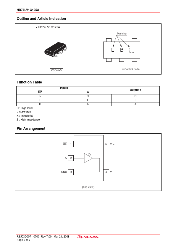
state output in a 5 pin package.
Output is disabled when the associated output enable (OE) input is high.
| Part number | HD74LV1G125A |
|---|---|
| Manufacturer | Renesas |
| File Size | 137.15 KB |
| Description | Bus Buffer Gate |
| Datasheet |
HD74LV1G125A Datasheet
|
|
|
|
Note: Below is a high-fidelity text extraction (approx. 800 characters) for HD74LV1G125A. For precise diagrams, and layout, please refer to the original PDF.
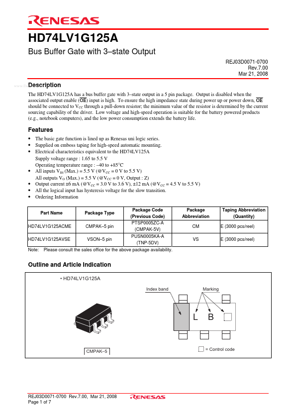
HD74LV1G125A Bus Buffer Gate with 3–state Output REJ03D0071-0700 Rev.7.00 Mar 21, 2008 www.DataSheet4U.net Description The HD74LV1G125A has a bus buffer gate with 3–state...
| Brand Logo | Part Number | Description | Manufacturer |
|---|---|---|---|
| HD74LV1G125A | Bus Buffer Gate | Hitachi Semiconductor |
| Part Number | Description |
|---|---|
| HD74LV1G126A | Bus Buffer Gate |
| HD74LV1G14A | Inverter |
| HD74LV1G02A | 2-input NOR Gate |
| HD74LV1G04A | Inverter |
| HD74LV1G08A | 2-input AND Gate |
| HD74LV1G66A | Analog Switch |
| HD74LV1G86A | 2-input ExclusiveOR Gate |
| HD74LV1GT00A | 2-input NAND Gate / CMOS Logic Level Shiftereg |
| HD74LV1GT02A | 2-input NOR Gate / CMOS Logic Level Shifter |
| HD74LV1GT04A | Inverter / CMOS Logic Level Shifter |