AP1286
Description
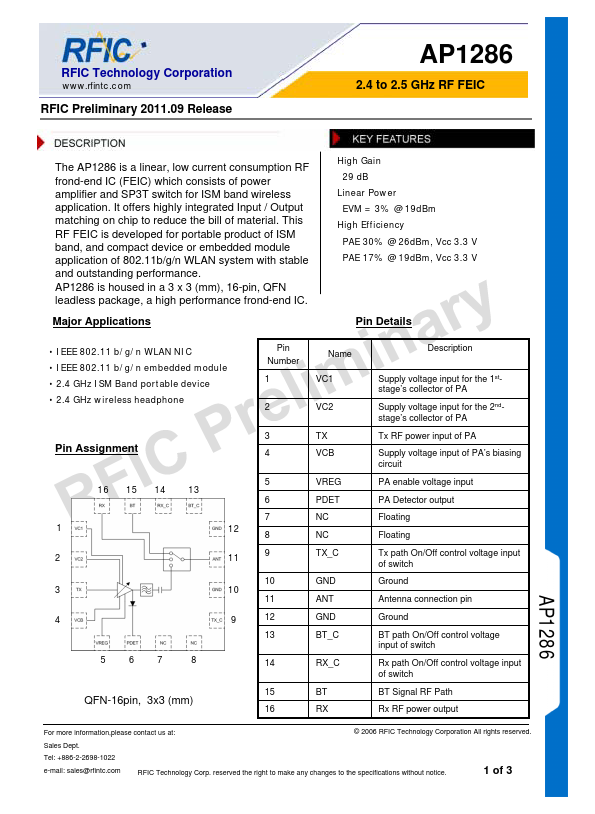
Supply voltage input for the 1ststage’s collector of PA Supply voltage input for the 2ndstage’s collector of PA Tx RF power input of PA Supply voltage input of PA’s biasing circuit PA enable voltage input PA Detector output Floating Floating Tx path On/Off control voltage input of switch Ground Antenna connection pin Ground BT path On/Off control voltage input of switch Rx path On/Off control voltage input of switch BT Signal RF Path Rx RF power output
For more information,please contact us at:
© 2006 RFIC Technology Corporation All rights reserved.
Sales Dept.
Tel: +886-2-2698-1022 e-mail: sales@rfintc.
RFIC Technology Corp. reserved the right to make any changes to the specifications without notice.
1 of 3
RFIC Technology Corporation
.rfintc.
RFIC Preliminary 2011.09 Release
2.4 to 2.5 GHz RF FEIC
Tx Chain Electrical Characteristics
VC1 = VC2 = VCB = 3.3V; VREG=2.85V; TX_C = H; BT_C =RX_C=L; RF Modulation = IEEE 802.11g, 54Mbps data rate, 64QAM...