RF3321
Features
- Differential Input and Output
- 31d B Maximum Voltage Gain
- -25d B Minimum Voltage Gain
- 5MHz to 65MHz Operation
- Sophisticated Power Management
- DOCSIS 1.1 RF pliant
Power Control
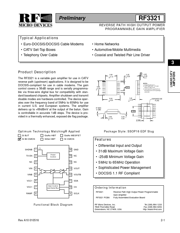
GND NC NC VOUT VOUTB SDA CS SCLK
15 14 13 12 11
Gain Control and Serial Bus
10 9
Ordering Information
RF3321 RF3321 PCBA Reverse Path High Output Power Programmable Gain Amplifier Fully Assembled Evaluation Board
Tel (336) 664 1233 Fax (336) 664 0454 http://.rfmd.
Functional Block Diagram
RF Micro Devices, Inc. 7628 Thorndike Road Greensboro, NC 27409, USA
Rev A10 010516
2-1
LINEAR CATV AMPLIFIERS
Product Description
Absolute Maximum Ratings Parameter
Supply Voltage (VCC1) Supply Voltage (VCC2) Input RF Level Operating Ambient Temperature Storage Temperature Humidity Maximum Power Dissipation Maximum TJ
Preliminary
Rating
-0.5 to +5.5 -0.5 to +7.5 12 -40 to +85 -40 to +150 80 0.5 150
Unit
VDC VDC d Bm °C °C % W °C Caution! ESD sensitive device.
RF Micro Devices believes...