Datasheet4U Logo Datasheet4U.com

QL4009 - Quick RAM

Description

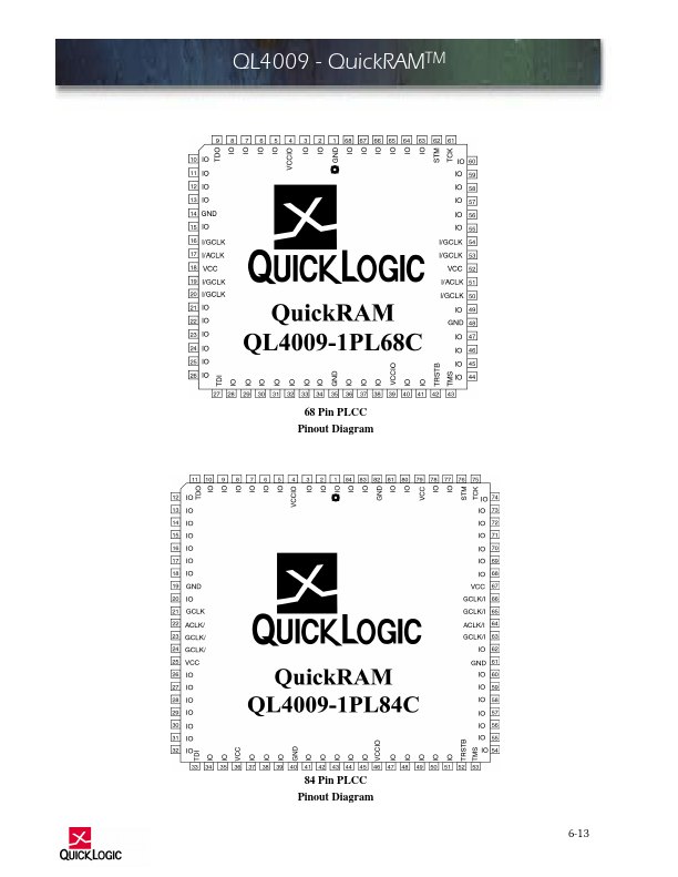
Pin TDI/RSI TRSTB/RRO TMS TCK TDO/RCO STM I/ACLK I/GCLK I I/O VCC VCCIO GND GND/THERM Function Test Data In for JTAG / RAM init.

Serial Data In Active low Reset for JTAG / RAM init.

reset out Test Mode Select for JTAG Test Clock for JTAG Test data out for JTAG / RAM init.

Features

  • up to 16 simultaneous inputs and 5 outs within a cell that can be fragmented into 5 independent cells. Each cell has a fan-in of 29 including register and control lines (see Figure 4). High Performance s s s s Input + logic cell + output total delays under 6 ns Data path speeds over 400 MHz counter speeds over 300 MHz FIFO speeds over 160 MHz QS A1 A2 A3 A4 A5 A6 OS OP B1 B2 C1 C2 MP MS D1 D2 E1 E2 NP NS F1 F2 F3 F4 F5 F6 AZ OZ WDATA WADDR RAM Module (1,152 bits) RDATA RADDR QZ NZ FZ.

📥 Download Datasheet

Datasheet Details

Part number QL4009
Manufacturer QuickLogic
File Size 500.69 KB
Description Quick RAM
Datasheet download datasheet QL4009 Datasheet
Other Datasheets by QuickLogic

Full PDF Text Transcription

Click to expand full text
QL4009 - QuickRAMTM 9,000 Usable PLD Gate QuickRAM ESP Combining Performance, Density, and Embedded RAM QL4009 - QuickRAM DEVICE HIGHLIGHTS Device Highlights High Performance & High Density s s 9,000 Usable PLD Gates with 82 I/Os 300 MHz 16-bit Counters, 400 MHz Datapaths, 160+ MHz FIFOs 0.35µm four-layer metal non-volatile CMOS process for smallest die sizes 8 RAM Blocks } 160 High Speed Logic Cells Interface s High Speed Embedded SRAM s FIGURE 1.
Published: |