PPM6N30V8
Description
The PPM6N30V8 uses advanced trench technology to provide excellent RDS(ON) and low gate charge. This device is suitable for use as a load switch or in PWM applications.
MOSFET Product Summary
VDS(V) -30
RDS(on)(mΩ)(Typ) 27 @ VGS=-10V
ID(A) -8
Feature
- High Power and current handing capability
- Lead free product is acquired
- Surface Mount Package
Applications
- PWM applications
- Load switch
- Power management
Absolute maximum rating@25℃
Rating
Drain-source Voltage
Gate-source Voltage
Drain Current
Total Power Dissipation
Junction and Storage Temperature Range
Thermal Characteristics
Rating
Thermal Resistance, Junction to Ambient1)
Thermal Resistance, Junction to Ambient2)
Thermal Resistance, Junction to Case
Rev.06.2
PPM6N30V8 P-Channel MOSFET
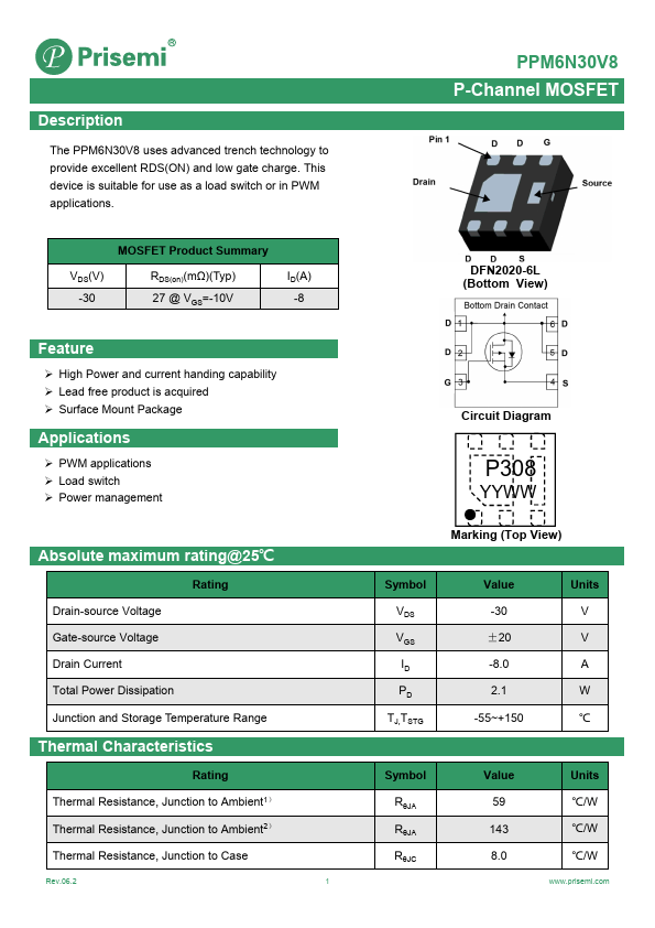
DFN2020-6L (Bottom View)
Circuit Diagram
P308
YYWW
Marking (Top View)
Symbol VDS VGS ID PD
TJ,TSTG
Value -30 ±20 -8.0 2.1
-55~+150
Units V V A W ℃
Symbol RθJA RθJA...