PNM8PN30V40
Description
The PNM8PN30V40 uses advanced trench technology to provide excellent RDS(ON), low gate charge. This device is suitable for use as a load switch or in PWM applications..
MOSFET Product Summary
VDS(V) 30
RDS(on)(mΩ) 4.5 @ VGS = 10V
ID(A) 40
PNM8PN30V40 N-Channel MOSFET
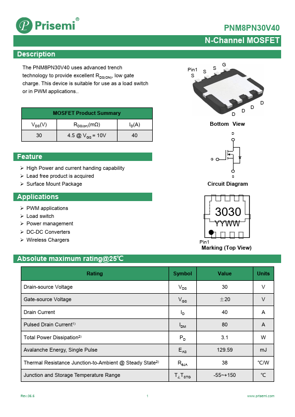
Pin1 S S G S
D D DD Bottom View
Feature
- High Power and current handing capability
- Lead free product is acquired
- Surface Mount Package
Applications
- PWM applications
- Load switch
- Power management
- DC-DC Converters
- Wireless Chargers
Absolute maximum rating@25℃
Rating
Drain-source Voltage
Gate-source Voltage
Drain Current
Pulsed Drain Current1)
Total Power Dissipation2)
Avalanche Energy, Single Pulse
Thermal Resistance Junction-to-Ambient @ Steady State2)
Junction and Storage Temperature Range
Circuit Diagram
YYWW
Pin1 Marking (Top View)
Symbol VDS VGS ID IDM PD EAS RθJA
TJ,TSTG
Value 30
±20 40 80...