PDNM6T20V7E
Description
The MOSFET provide the best bination of fast switching, low on-resistance and cost-effectiveness.
VDS(V) 20
MOSFET Product Summary
RDS(on)(mΩ)
ID(A)
16@ VGS=4.5V
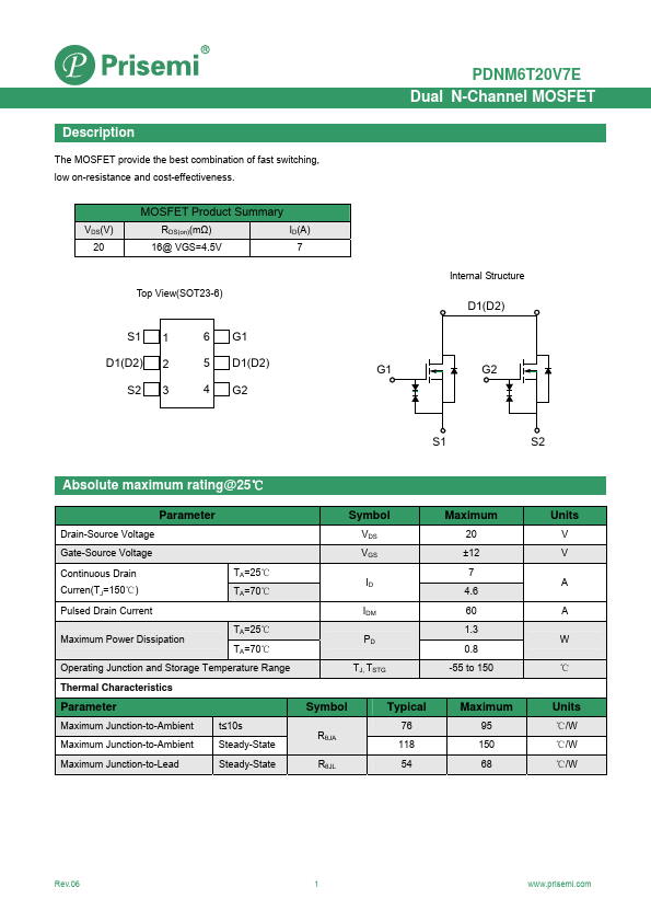
Top View(SOT23-6)
S1 1 D1(D2) 2
S2 3
6 G1 5 D1(D2) 4 G2
PDNM6T20V7E Dual N-Channel MOSFET
Internal Structure
D1(D2)
G1
G2
S1
S2
Absolute maximum rating@25℃
Parameter
Drain-Source Voltage
Gate-Source Voltage
Continuous Drain Curren(TJ=150℃) Pulsed Drain Current
TA=25℃ TA=70℃
Maximum Power Dissipation
TA=25℃ TA=70℃
Operating Junction and Storage Temperature Range
Thermal Characteristics
Parameter
Maximum Junction-to-Ambient t≤10s
Maximum Junction-to-Ambient
Steady-State
Maximum Junction-to-Lead
Steady-State
Symbol
VDS VGS ID IDM PD TJ, TSTG
Symbol
RθJA...