Datasheet Details
| Part number | A3S12D40ETP |
|---|---|
| Manufacturer | Powerchip |
| File Size | 2.10 MB |
| Description | 512Mb DDR SDRAM |
| Datasheet |
 A3S12D40ETP Datasheet A3S12D40ETP Datasheet
|
|
|
Download the A3S12D40ETP datasheet PDF. This datasheet also includes the A3S12D30ETP variant, as both parts are published together in a single manufacturer document.
| Part number | A3S12D40ETP |
|---|---|
| Manufacturer | Powerchip |
| File Size | 2.10 MB |
| Description | 512Mb DDR SDRAM |
| Datasheet |
A3S12D40ETP Datasheet
|
|
|
|
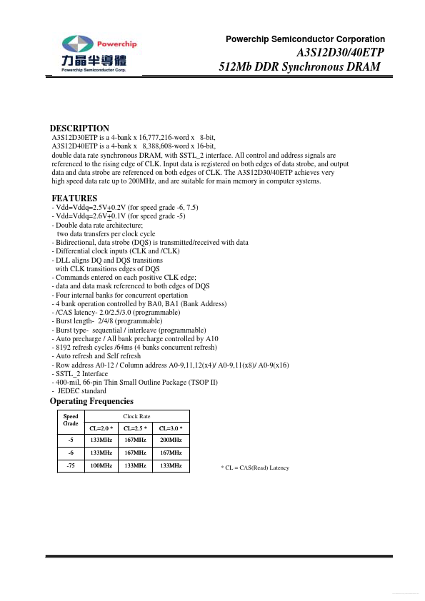
A3S12D30ETP is a 4-bank x 16,777,216-word x 8-bit, A3S12D40ETP is a 4-bank x 8,388,608-word x 16-bit, double data rate synchronous DRAM, with SSTL_2 interface.
All control and address signals are referenced to the rising edge of CLK.
Input data is registered on both edges of data strobe, and output data and data strobe are referenced on both edges of CLK.
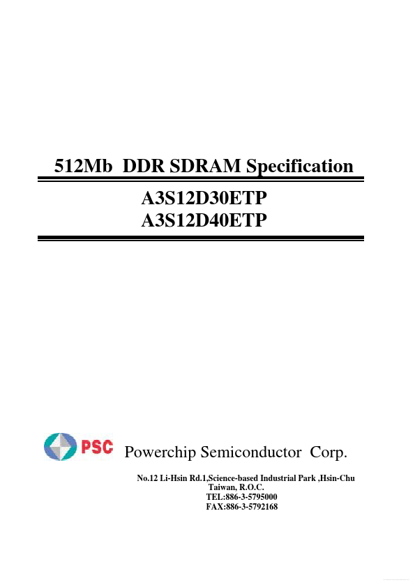
512Mb DDR SDRAM Specification A3S12D30ETP A3S12D40ETP Powerchip Semiconductor Corp.
No.12 Li-Hsin Rd.1,Science-based Industrial Park ,Hsin-Chu Taiwan, R.O.C.
TEL:886-3-5795000 FAX:886-3-5792168 Free Datasheet http://www.datasheet4u.net/ Powerchip Semiconductor Corporation A3S12D30/40ETP 512Mb DDR Synchronous DRAM PRELIMINARY Some of contents are subject to change without notice.
| Part Number | Description |
|---|---|
| A3S12D30ETP | 512Mb DDR SDRAM |