The following content is an automatically extracted verbatim text
from the original manufacturer datasheet and is provided for reference purposes only.
View original datasheet text
INTEGRATED CIRCUITS
74F808, 74F1808 Hex 2-input AND drivers
Product specification IC15 Data Handbook 1991 Jan 02
Philips Semiconductors
Philips Semiconductors
Product specification
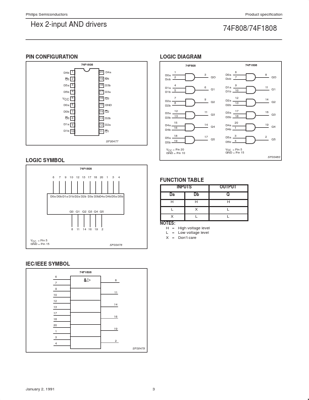
Hex 2-input AND drivers
74F808/74F1808
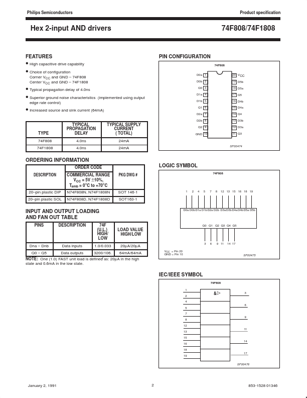
FEATURES
• High capacitive drive capability • Choice of configuration • Typical propagation delay of 4.0ns • Superior ground noise characteristics
edge rate control) Corner VCC and GND – 74F808 Center VCC and GND – 74F1808
PIN CONFIGURATION
74F808 D0a 1 D0b 2 Q0 3 20 VCC 19 D5b 18 D5a 17 Q5 16 D4b 15 D4a 14 Q4 13 D3b 12 D3a 11 Q3
(implemented using output
D1a 4 D1b 5 Q1 6 D2a 7 D2b 8
• Increased source and sink current (64mA)
TYPICAL PROPAGATION DELAY 4.0ns 4.
 74F808 Datasheet