2N2369A
FEATURES
- Low current (max. 200 m A)
- Low voltage (max.15 V).
APPLICATIONS
- High-speed saturated switching and high frequency amplifier applications.
DESCRIPTION
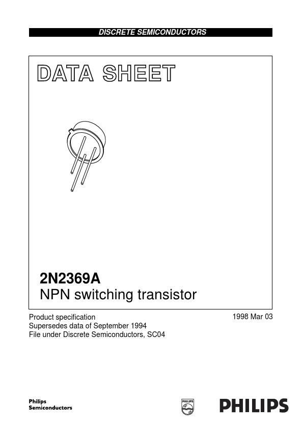
NPN switching transistor in a TO-18 metal package.
PINNING
PIN 1 2 3
DESCRIPTION emitter base collector, connected to case handbook, halfpa1ge 2
MAM264
3 1
Fig.1 Simplified outline (TO-18) and symbol.
QUICK REFERENCE DATA
SYMBOL
PARAMETER
VCBO VCEO IC Ptot h FE collector-base voltage collector-emitter voltage collector current (DC) total power dissipation DC current gain f T transition frequency toff turn-off time
CONDITIONS open emitter open base
Tamb ≤ 25 °C IC = 10 m A; VCE = 350 m V IC = 10 m A; VCE = 1 V IC = 10 m A; VCE = 10 V; f = 100 MHz ICon = 10 m A; IBon = 3 m A; IBoff =
- 1.5 m A
MIN.
- -
- - 40
- 500
- MAX.
40 15 200 360
- 120
- 30
UNIT V V m A m W
MHz ns
1998 Mar 03
Philips Semiconductors
NPN switching transistor
Product specification
LIMITING VALUES In accordance with the Absolute...