Datasheet Details
| Part number | PI90LV211 |
|---|---|
| Manufacturer | Pericom Semiconductor Corporation |
| File Size | 185.52 KB |
| Description | 1:6 Differential Clock Distribution Chip |
| Datasheet |
 PI90LV211 Datasheet PI90LV211 Datasheet
|
|
|
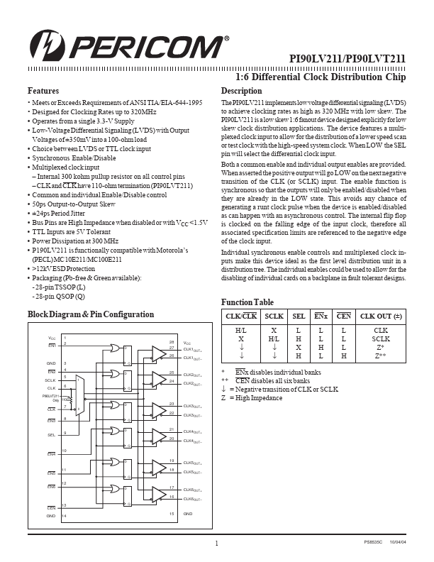
The PI90LV211 implements low voltage differential signaling (LVDS) to achieve clocking rates as high as 320 MHz with low skew.
The PI90LV211 is a low skew 1:6 fanout device designed explicitly for low skew clock distribution applications.
| Part number | PI90LV211 |
|---|---|
| Manufacturer | Pericom Semiconductor Corporation |
| File Size | 185.52 KB |
| Description | 1:6 Differential Clock Distribution Chip |
| Datasheet |
PI90LV211 Datasheet
|
|
|
|
| Part Number | Description | Manufacturer |
|---|---|---|
| PI90LV01 | SOTiny LVDS High-Speed Differential Line Driver | Pericom Semiconductor |
| PI90LV01 | SOTiny LVDS High-Speed Differential Line Driver | DIODES |
| PI90LV017A | 3V LVDS High-Speed Differential Line Drivers | Pericom Semiconductor |
| PI90LV018A | 3V LVDS High-Speed Differential Line Drivers | Pericom Semiconductor |
| PI90LV019 | Single Bus LVDS Transceiver | Pericom Semiconductor |
| Part Number | Description |
|---|---|
| PI90LV386 | High-Speed Differential Line Receivers |
| PI90LV387 | High-Speed Differential Line Drivers |
| PI90LVB387 | High-Speed Differential Line Drivers |
| PI90LVT211 | 1:6 Differential Clock Distribution Chip |
| PI90LVT386 | High-Speed Differential Line Receivers |