Note: Below is a high-fidelity text extraction (approx. 800 characters) for
K3559. For precise diagrams, and layout, please refer to the original PDF.
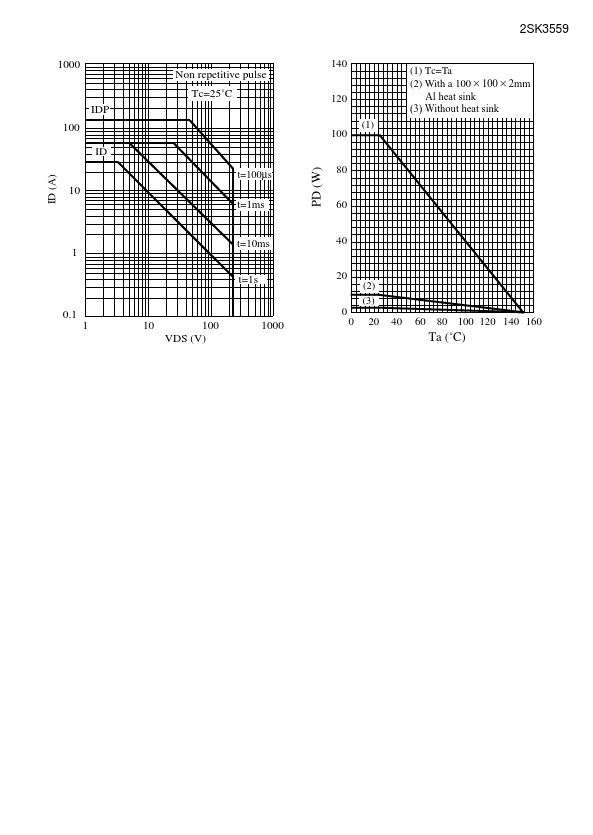
Silicon MOSFET 2SK3559 N-channel enhancement mode MOSFET High speed switching Absolute Maximum Ratings Parameter Drain-Source breakdown voltage Gate-Source voltage Drain ...
View more extracted text
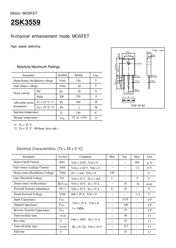
gs Parameter Drain-Source breakdown voltage Gate-Source voltage Drain current DC Pulse Allowable power Tc = 25 °C *1 dissipation Ta = 25 °C *2 Junction temperature Storage temperature Symbol VDSS VGSS ID IDP PD PD Tj Tstg Rating 230 30 30 120 100 3 150 -55 to +150 *1 : Tc = 25 °C *2 : Ta = 25 °C (Without heat sink ) Unit V V A A W W °C °C 16.2±0.5 (3.2) (2.3) Solder Dip 21.0±0.5 15.0±0.2 (0.7) 15.0±0.3 11.0±0.2 Unit : mm 5.0±0.2 (3.2) φ 3.2±0.1 2.0±0.2 1.1±0.1 2.0±0.1 0.6±0.2 5.45±0.3 10.9±0.
 K3559 Datasheet