1.1±0.1 0.75±0.1
0.85±0.1 0.4±0.1
2.3±0.2
4.6±0.4 2
s
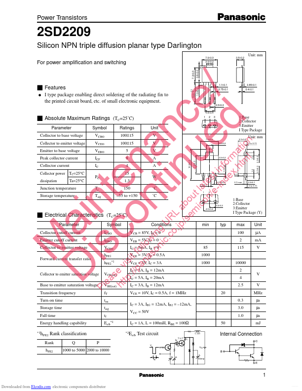
Absolute Maximum Ratings (TC=25˚C)
Parameter Symbol VCBO VCEO VEBO ICP IC 100±15 100±15 5 8 4
1
3
Ratings
Unit V V V A A
1:Base 2:Collector 3:Emitter I Type Package Unit: mm
0 to 0.15
Collector to emitter voltage Emitter to base voltage Peak collector current Collector current
Collector power TC=25°C dissipation Ta=25°C Junction temperature Storage temperature
PC Tj
Tstg
s
Electrical Characteristics (TC=25˚C)
Parameter Symbol.
Note: Below is a high-fidelity text extraction (approx. 800 characters) for
D2209. For precise diagrams, tables, and layout, please refer to the original PDF.
View original datasheet text
Power Transistors
2SD2209
Silicon NPN triple diffusion planar type Darlington
7.0±0.3 3.5±0.2
Unit: mm
For power amplification and switching
7.2±0.3 0.8±0.2
3.0±0.2
1.0±0.2
M Di ain sc te on na tin nc ue e/ d
q
I type package enabling direct soldering of the radiating fin to the printed circuit board, etc. of small electronic equipment.
10.0 –0.
+0.3
s Features
1.1±0.1 0.75±0.1
0.85±0.1 0.4±0.1
2.3±0.2
4.6±0.4 2
s
Absolute Maximum Ratings (TC=25˚C)
Parameter Symbol VCBO VCEO VEBO ICP IC 100±15 100±15 5 8 4
1
3
Ratings
Unit V V V A A
1:Base 2:Collector 3:Emitter I Type Package Unit: mm
0 to 0.
 D2209 Datasheet