Click to expand full text
PG 12232-B
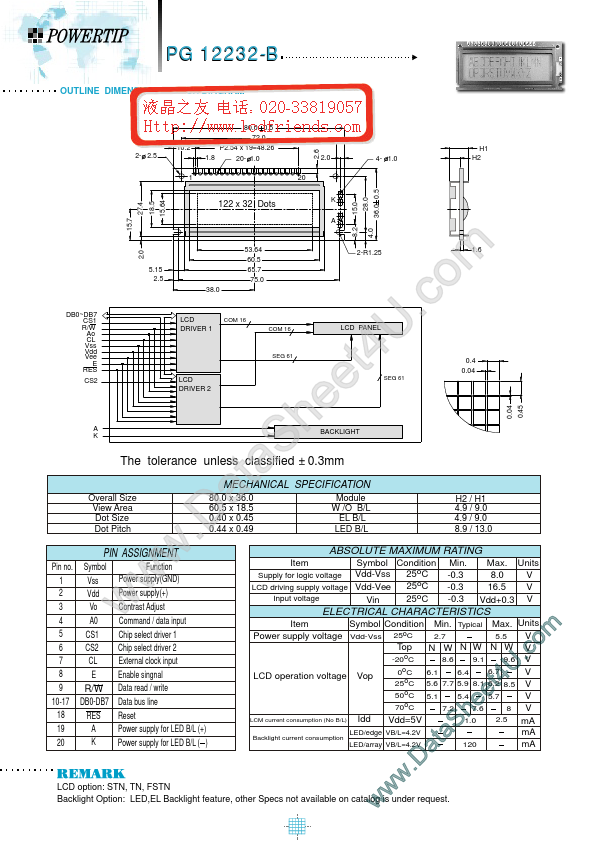
OUTLINE DIMENSION & BLOCK DIAGRAM
2- 2.5 1
1.8
2.6
10.2
80.0 0.5 72.0 P2.54 x 19=48.26 20- 1.0 20
2.0
4- 1.0
H1 H2
15.64
15.7
27.4
18.5
122 x 32 Dots
A 8.2
DB0~DB7 CS1 R/W Ao CL Vss Vdd Vee E RES CS2
A K
Overall Size View Area Dot Size Dot Pitch
PIN ASSIGNMENT
Pin no. 1 2 3 4 5 6 7 8 9 10-17 18 19 20 Symbol Vss Vdd Vo A0 CS1 CS2 CL E R/W DB0-DB7 RES A K
Function Power supply(GND) Power supply(+) Contrast Adjust Command / data input Chip select driver 1 Chip select driver 2 External clock input Enable singnal Data read / write Data bus line Reset Power supply for LED B/L (+) Power supply for LED B/L ( )
m o .c U 4 t e e h S a t a .D w w w
53.64 60.5 2.0 2-R1.25 1.6 5.15 2.5 65.7 75.0 38.0 LCD DRIVER 1
COM 16 COM 16
LCD PANEL
SEG 61
4.0
15.0 28.0
K
36.
 pg12232b Datasheet