NLAS323
Features
- On Resistance is 20 W Typical at 5.0 V
- Matching is < 1.0 W Between Sections
- 2.0 to 6.0 V Operating Range
- Ultra Low < 5.0 p C Charge Injection
- Ultra Low Leakage < 1.0 n A at 5.0 V, 25 C
- Wide Bandwidth > 200 MHz,
- 3.0 d B
- 2000 V ESD (Human Body Model)
- Ron Flatness $6.0 W at 5.0 V
- US8 Package
- Independent, Positive Enable
- These Devices are Pb- Free, Halogen Free/BFR Free and are Ro HS pliant
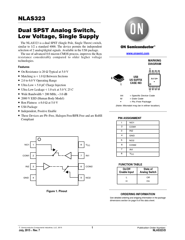
NO1 1 1 2
IN2 3 GND 4
8 VCC 7 IN1 6 2 5 NO2
.onsemi.
MARKING DIAGRAM 8
8 US8 US SUFFIX
1 CASE 493
A4 MG G
A4 = Specific Device Code M = Date Code G = Pb- Free Package
(Note: Microdot may be in either location)
PIN ASSIGNMENT 1 NO1 2 1 3 IN2 4 GND 5 NO2 6 2 7 IN1 8 VCC
FUNCTION TABLE
On/Off Enable Input
State of Analog Switch
L Off H On
Figure 1. Pinout
ORDERING INFORMATION
See detailed ordering and shipping information in the package dimensions section on page 8 of this data sheet.
© Semiconductor ponents Industries, LLC, 2015
July, 2015
- Rev....