MMBD2837LT1
Features
- Pb- Free Packages are Available http://onsemi.
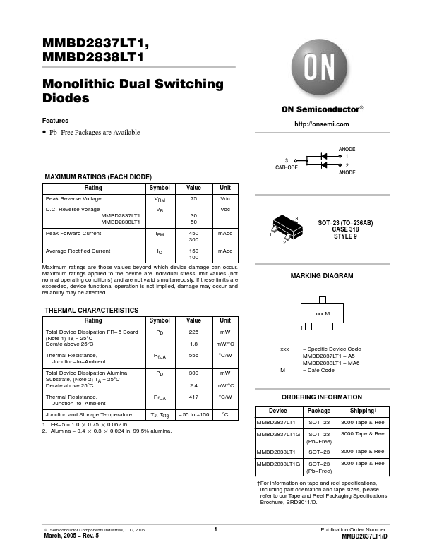
3 CATHODE
ANODE 1 2 ANODE
MAXIMUM RATINGS (EACH DIODE)
Rating Peak Reverse Voltage D.C. Reverse Voltage MMBD2837LT1 MMBD2838LT1 Peak Forward Current Average Rectified Current IFM IO Symbol VRM VR 30 50 450 300 150 100 m Adc m Adc
1 2
Value 75
Unit Vdc Vdc
SOT- 23 (TO- 236AB) CASE 318 STYLE 9
Maximum ratings are those values beyond which device damage can occur. Maximum ratings applied to the device are individual stress limit values (not normal operating conditions) and are not valid simultaneously. If these limits are exceeded, device functional operation is not implied, damage may occur and reliability may be affected.
MARKING DIAGRAM
THERMAL CHARACTERISTICS
Rating Total Device Dissipation FR- 5 Board (Note 1) TA = 25°C Derate above 25°C Thermal Resistance, Junction- to- Ambient Total Device Dissipation Alumina Substrate, (Note 2) TA = 25°C Derate above 25°C Thermal Resistance, Junction- to- Ambient Junction and Storage...