Click to expand full text
VN0610LL
FET Transistor
N−Channel — Enhancement
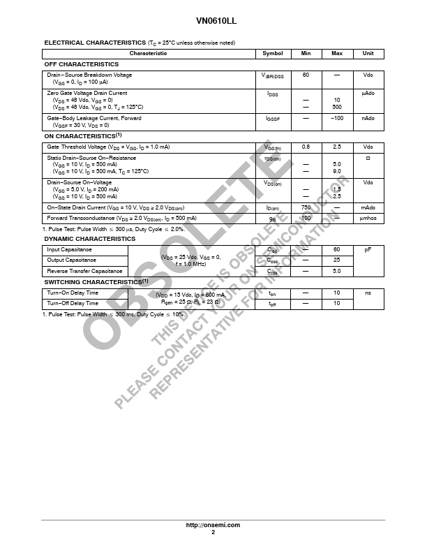
MAXIMUM RATINGS
Rating
Drain −Source Voltage
Drain −Gate Voltage (RGS = 1 MΩ)
Gate −Source Voltage − Continuous − Non−repetitive (tp ≤ 50 μs)
Drain Current Continuous Pulsed
Total Power Dissipation @ TA = 25°C Derate above 25°C
Operating and Storage Temperature Range
THERMAL CHARACTERISTICS
Characteristics
Thermal Resistance, Junction to Ambient
Maximum Lead Temperature for Soldering Purposes, 1/16” from case for 10 seconds
Symbol VDSS VDGR
Value 60 60
Unit Vdc Vdc
VGS VGSM
ID IDM PD
TJ, Tstg
± 20 ± 40
190 1000 400 3.2 −55 to +150
Vdc Vpk mAdc
mW mW/°C
°C
Symbol RθJA
TL
Max 312.5
300
Unit °C/W
°C
http://onsemi.
 VN0610LL Datasheet