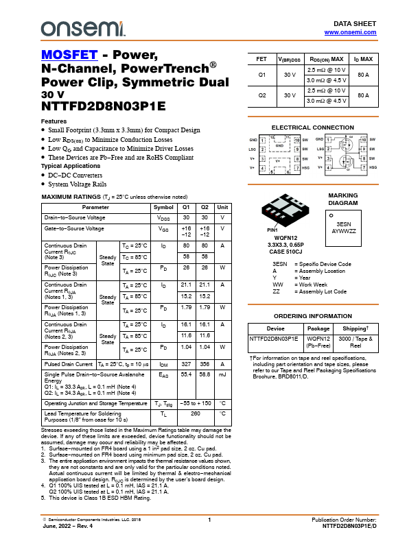
NTTFD2D8N03P1E
Features
- Small Footprint (3.3mm x 3.3mm) for pact Design
- Low RDS(on) to Minimize Conduction Losses
- Low QG and Capacitance to Minimize Driver Losses
- These Devices are Pb- Free and are Ro HS pliant
Typical Applications
- DC- DC Converters
- System Voltage Rails
MAXIMUM RATINGS (TJ = 25°C unless otherwise noted)
Parameter
Symbol Q1
Q2 Unit
Drain- to- Source Voltage Gate- to- Source Voltage
VDSS
VGS +16 +16 V
- 12
- 12
Continuous Drain
TC = 25°C
Current Rq JC (Note 3)
Steady TC = 85°C
State
Power Dissipation Rq JC (Note 3)
TA = 25°C
80 80 A 58 58 26 26 W
Continuous Drain
TA = 25°C
21.1 21.1 A
Current Rq JA (Notes 1, 3)
Steady TA = 85°C
15.2 15.2
State
Power Dissipation Rq JA (Notes 1, 3)
TA = 25°C
1.79 1.79...