Click to expand full text
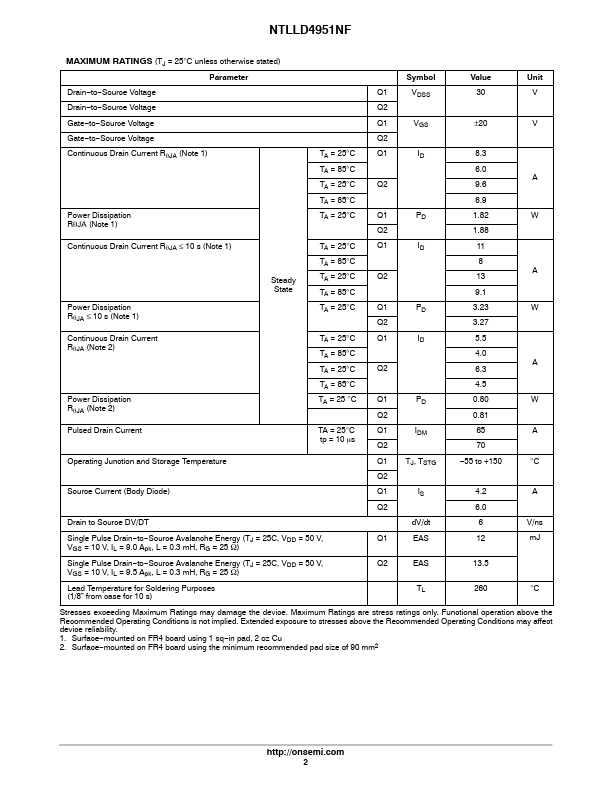
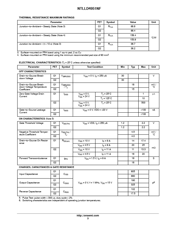
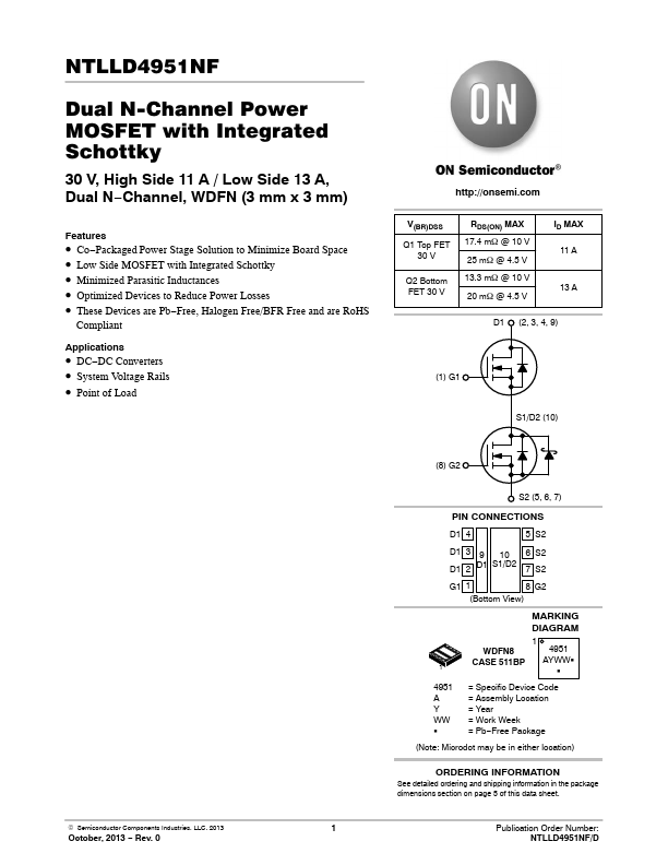
NTLLD4951NF
Dual N-Channel Power MOSFET with Integrated Schottky
30 V, High Side 11 A / Low Side 13 A, Dual N−Channel, WDFN (3 mm x 3 mm)
Features
• Co−Packaged Power Stage Solution to Minimize Board Space • Low Side MOSFET with Integrated Schottky • Minimized Parasitic Inductances • Optimized Devices to Reduce Power Losses • These Devices are Pb−Free, Halogen Free/BFR Free and are RoHS
Compliant
Applications
• DC−DC Converters • System Voltage Rails • Point of Load
http://onsemi.com
V(BR)DSS
Q1 Top FET 30 V
Q2 Bottom FET 30 V
RDS(ON) MAX 17.4 mW @ 10 V 25 mW @ 4.5 V 13.3 mW @ 10 V 20 mW @ 4.5 V
ID MAX 11 A
13 A
D1 (2, 3, 4, 9)
(1) G1
S1/D2 (10)
© Semiconductor Components Industries, LLC, 2013
October, 2013 − Rev.
 NTLLD4951NF Datasheet