Click to expand full text
NTJD1155L
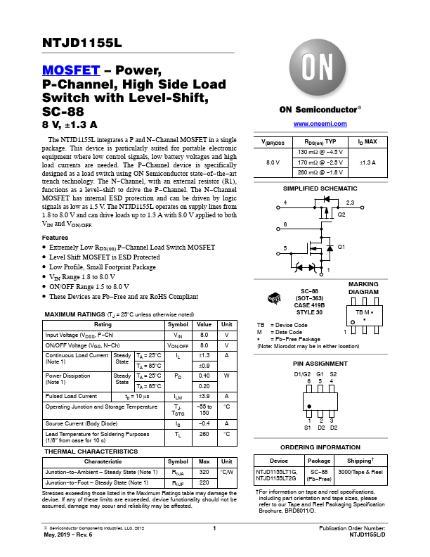
MOSFET – Power, P-Channel, High Side Load Switch with Level-Shift, SC-88
8 V, +1.3 A
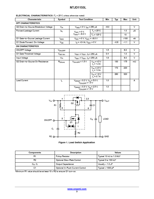
The NTJD1155L integrates a P and N−Channel MOSFET in a single package. This device is particularly suited for portable electronic equipment where low control signals, low battery voltages and high load currents are needed. The P−Channel device is specifically designed as a load switch using ON Semiconductor state−of−the−art trench technology. The N−Channel, with an external resistor (R1), functions as a level−shift to drive the P−Channel. The N−Channel MOSFET has internal ESD protection and can be driven by logic signals as low as 1.5 V. The NTJD1155L operates on supply lines from 1.8 to 8.0 V and can drive loads up to 1.3 A with 8.0 V applied to both VIN and VON/OFF.
 NTJD1155L Datasheet