Click to expand full text
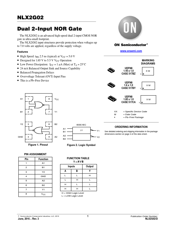
NLX2G02
Dual 2-Input NOR Gate
The NLX2G02 is an advanced high-speed dual 2-input CMOS NOR gate in ultra-small footprint.
The NLX2G02 input structures provide protection when voltages up to 7.0 volts are applied, regardless of the supply voltage.
Features
• High Speed: tPD 2.5 ns (typical) at VCC = 5.0 V • Designed for 1.65 V to 5.5 V VCC Operation • Low Power Dissipation: ICC = 1 mA (Max) at TA = 25°C • 24 mA Balanced Output Sink and Source Capability • Balanced Propagation Delays • Overvoltage Tolerant (OVT) Input Pins • This is a Pb−Free Device
A1 1
8 VCC
www.onsemi.com
UDFN8 1.45 x 1.0 CASE 517BZ
MARKING DIAGRAMS
XM 1
UDFN8
1.6 x 1.0
XM
CASE 517BY 1
UDFN8
1.95 x 1.0
XM
CASE 517CA 1
B1 2
7 Y1
Y2 3
6 B2
GND 4
5 A2
Figure 1.
 NLX2G02 Datasheet