Click to expand full text
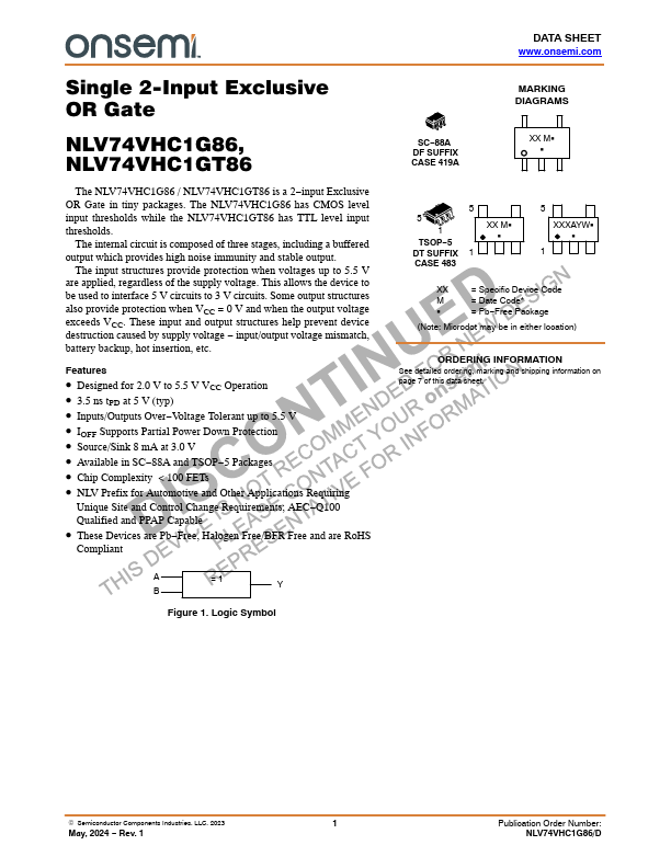
Single 2-Input Exclusive OR Gate
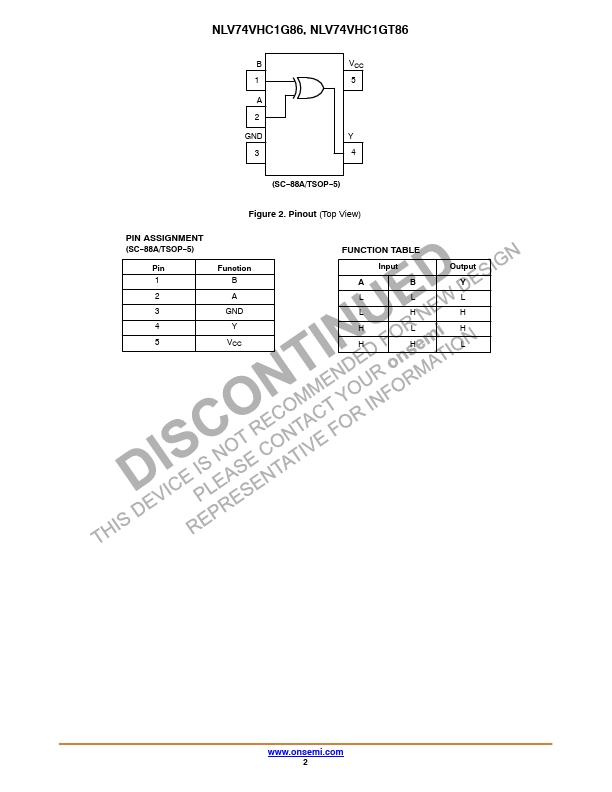
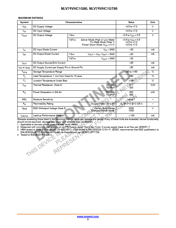
NLV74VHC1G86, NLV74VHC1GT86
The NLV74VHC1G86 / NLV74VHC1GT86 is a 2−input Exclusive OR Gate in tiny packages. The NLV74VHC1G86 has CMOS level input thresholds while the NLV74VHC1GT86 has TTL level input thresholds.
The internal circuit is composed of three stages, including a buffered output which provides high noise immunity and stable output.
The input structures provide protection when voltages up to 5.5 V are applied, regardless of the supply voltage. This allows the device to be used to interface 5 V circuits to 3 V circuits. Some output structures also provide protection when VCC = 0 V and when the output voltage exceeds VCC.
 NLV74VHC1GT86 Datasheet