Click to expand full text
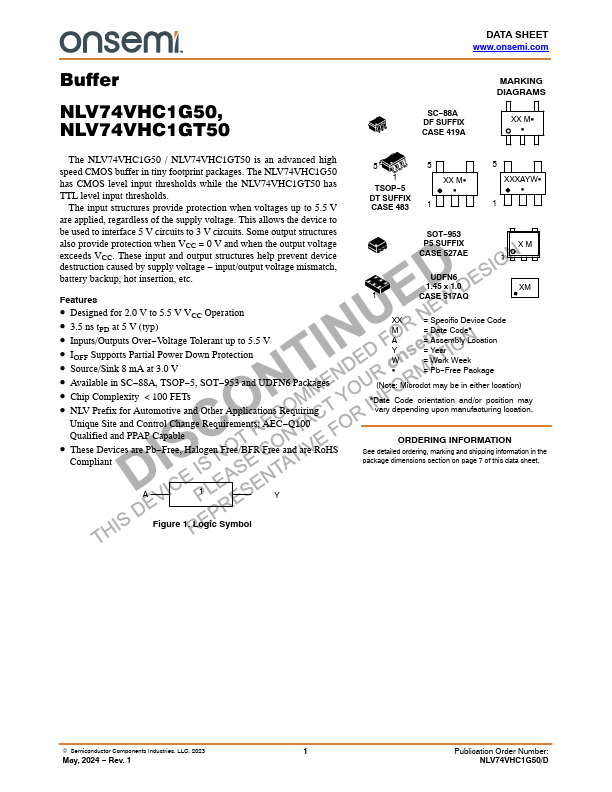
Buffer
NLV74VHC1G50, NLV74VHC1GT50
The NLV74VHC1G50 / NLV74VHC1GT50 is an advanced high speed CMOS buffer in tiny footprint packages. The NLV74VHC1G50 has CMOS level input thresholds while the NLV74VHC1GT50 has TTL level input thresholds.
The input structures provide protection when voltages up to 5.5 V are applied, regardless of the supply voltage. This allows the device to be used to interface 5 V circuits to 3 V circuits. Some output structures also provide protection when VCC = 0 V and when the output voltage exceeds VCC. These input and output structures help prevent device destruction caused by supply voltage − input/output voltage mismatch, battery backup, hot insertion, etc.
Features
• Designed for 2.0 V to 5.5 V VCC Operation • 3.
 NLV74VHC1GT50 Datasheet