Click to expand full text
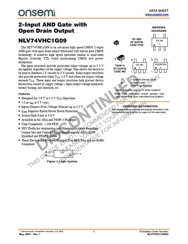
2-Input AND Gate with Open Drain Output
NLV74VHC1G09
The NLV74VHC1G09 is an advanced high speed CMOS 2−input AND gate with open drain output fabricated with silicon gate CMOS technology. It achieves high speed operation similar to equivalent Bipolar Schottky TTL while maintaining CMOS low power dissipation.
The input structures provide protection when voltages up to 5.5 V are applied, regardless of the supply voltage. This allows the device to be used to interface 5 V circuits to 3 V circuits. Some output structures also provide protection when VCC = 0 V and when the output voltage exceeds VCC. These input and output structures help prevent device destruction caused by supply voltage − input/output voltage mismatch, battery backup, hot insertion, etc.
Features
• Designed for 2.0 V to 5.
 NLV74VHC1G09 Datasheet