Datasheet4U Logo Datasheet4U.com

NLSX4402 - 2-Bit 20 Mb/s Dual-Supply Level Translator

Datasheet Summary

Description

VCC VL GND VCC Supply Voltage VL Supply Voltage Ground EN I/O VCCn I/O VLn Output Enable, Referenced to VL I/O Port, Referenced to VCC I/O Port, Referenced to VL FUNCTION TABLE EN L H Operating Mode Hi Z I/O Buses Connected www.onsemi.com 2 NLSX4402 MAXIMUM RATINGS Symbol Paramete

Features

  • VL can be Less than, Greater than or Equal to VCC.
  • Wide VCC Operating Range: 1.5 V to 5.5 V Wide VL Operating Range: 1.5 V to 5.5 V.
  • Enable Input and I/O Pins are Overvoltage Tolerant (OVT) to 5.5 V.
  • Non.
  • preferential Powerup Sequencing.
  • Power.
  • Off Protection.
  • Small Space Saving Package: 1.45 mm x 1.0 mm UDFN8 Package.
  • These Devices are Pb.
  • Free, Halogen Free/BFR Free and are RoHS Compliant Typical.

📥 Download Datasheet

Datasheet preview – NLSX4402

Datasheet Details

Part number NLSX4402
Manufacturer ON Semiconductor
File Size 105.15 KB
Description 2-Bit 20 Mb/s Dual-Supply Level Translator
Datasheet download datasheet NLSX4402 Datasheet
Additional preview pages of the NLSX4402 datasheet.
Other Datasheets by ON Semiconductor

Full PDF Text Transcription

Click to expand full text
NLSX4402 2-Bit 20 Mb/s Dual-Supply Level Translator 
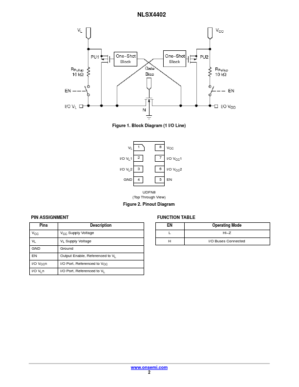
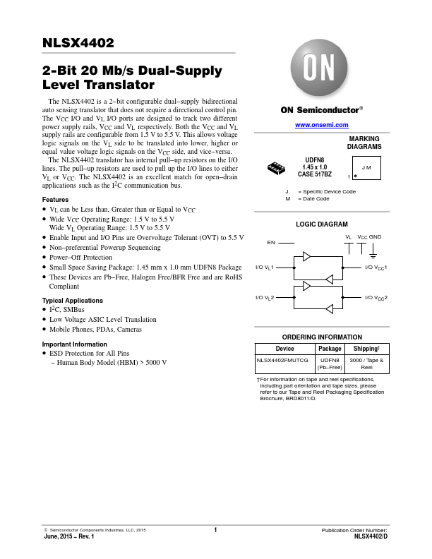
The NLSX4402 is a 2−bit configurable dual−supply bidirectional auto sensing translator that does not require a directional control pin. The VCC I/O and VL I/O ports are designed to track two different power supply rails, VCC and VL respectively. Both the VCC and VL supply rails are configurable from 1.5 V to 5.5 V. This allows voltage logic signals on the VL side to be translated into lower, higher or equal value voltage logic signals on the VCC side, and vice−versa. The NLSX4402 translator has internal pull−up resistors on the I/O lines. The pull−up resistors are used to pull up the I/O lines to either VL or VCC. The NLSX4402 is an excellent match for open−drain applications such as the I2C communication bus.
Published: |