Click to expand full text
NLSX4401DFT2G
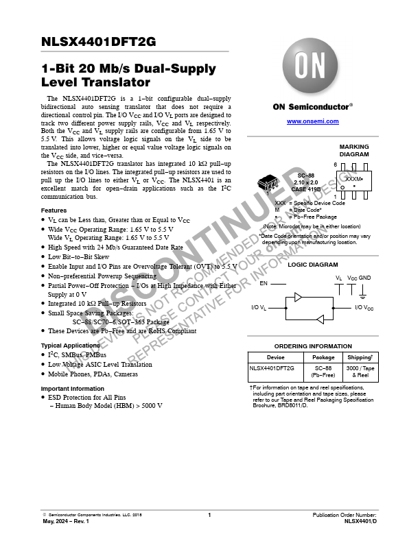
1-Bit 20 Mb/s Dual-Supply Level Translator
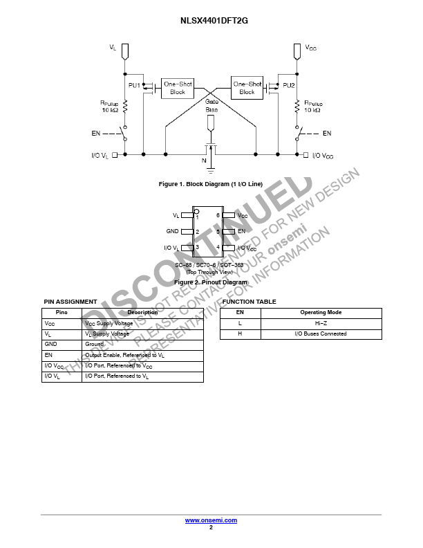
The NLSX4401DFT2G is a 1−bit configurable dual−supply bidirectional auto sensing translator that does not require a directional control pin. The I/O VCC and I/O VL ports are designed to track two different power supply rails, VCC and VL respectively. Both the VCC and VL supply rails are configurable from 1.65 V to 5.5 V. This allows voltage logic signals on the VL side to be translated into lower, higher or equal value voltage logic signals on the VCC side, and vice−versa.
The NLSX4401DFT2G translator has integrated 10 kW pull−up resistors on the I/O lines. The integrated pull−up resistors are used to pull up the I/O lines to either VL or VCC.
 NLSX4401DFT2G Datasheet