Datasheet4U Logo Datasheet4U.com

NLSF3T125 - Quad Bus Buffer

Datasheet Summary

Features

  • High Speed: tPD = 3.8 ns (Typ) at VCC = 5.0 V.
  • Low Power Dissipation: ICC = 4.0 mA (Max) at TA = 25°C.
  • TTL.
  • Compatible Inputs: VIL = 0.8 V; VIH = 2.0 V.
  • Power Down Protection Provided on Inputs.
  • Balanced Propagation Delays.
  • Designed for 2.0 V to 5.5 V Operating Range.
  • Low Noise: VOLP = 0.8 V (Max).
  • Pin and Function Compatible with Other Standard Logic Families.
  • Latchup Performance Exceeds 300 mA.
  • ES.

📥 Download Datasheet

Datasheet preview – NLSF3T125

Datasheet Details

Part number NLSF3T125
Manufacturer ON Semiconductor
File Size 209.04 KB
Description Quad Bus Buffer
Datasheet download datasheet NLSF3T125 Datasheet
Additional preview pages of the NLSF3T125 datasheet.
Other Datasheets by ON Semiconductor

Full PDF Text Transcription

Click to expand full text
NLSF3T125 Quad Bus Buffer with 3−State Control Inputs 
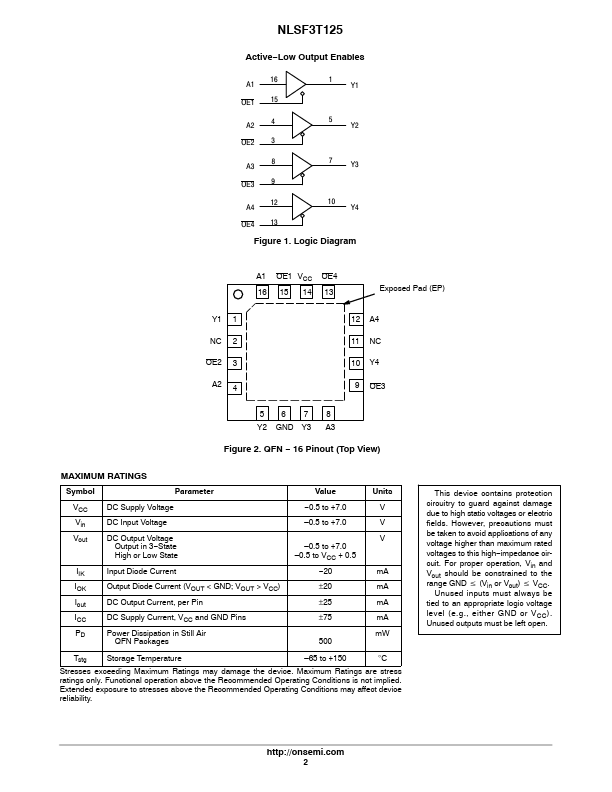
The NLSF3T125 is a high speed CMOS quad bus buffer fabricated with silicon gate CMOS technology. It achieves high speed operation similar to equivalent Bipolar Schottky TTL while maintaining CMOS low power dissipation. The NLSF3T125 requires the 3−state control input (OE) to be set High to place the output into the high impedance state. The T125 inputs are compatible with TTL levels. This device can be used as a level converter for interfacing 3.3 V to 5.0 V, because it has full 5.0 V CMOS level output swings. The NLSF3T125 input structures provide protection when voltages between 0 V and 5.5 V are applied, regardless of the supply voltage. The output structures also provide protection when VCC = 0 V.
Published: |