NDP08N50Z
Features
- -
- -
Low ON Resistance Low Gate Charge 100% Avalanche Tested These Devices are Pb- Free and are Ro HS pliant
VDSS 500 V http://onsemi.
RDS(ON) (TYP) @ 3.6 A 0.69 W
ABSOLUTE MAXIMUM RATINGS (TC = 25°C unless otherwise noted)
Rating Drain- to- Source Voltage Continuous Drain Current Rq JC Continuous Drain Current Rq JC TA = 100°C Pulsed Drain Current, VGS @ 10 V Power Dissipation Gate- to- Source Voltage Single Pulse Avalanche Energy, ID = 7.5 A ESD (HBM) (JESD 22- A114) RMS Isolation Voltage (t = 0.3 sec., R.H. ≤ 30%, TA = 25°C) (Figure 14) Peak Diode Recovery Continuous Source Current (Body Diode) Maximum Temperature for Soldering Leads Operating Junction and Storage Temperature Range Symbol VDSS ID ID IDM PD VGS EAS Vesd VISO 4500 NDF08N50Z NDP08N50Z Unit V 7.5 4.7 30 125 30 190 3500 A A A W V m J V V 500 7.5 (Note 1) 4.7 (Note 1) 30 (Note 1) 31
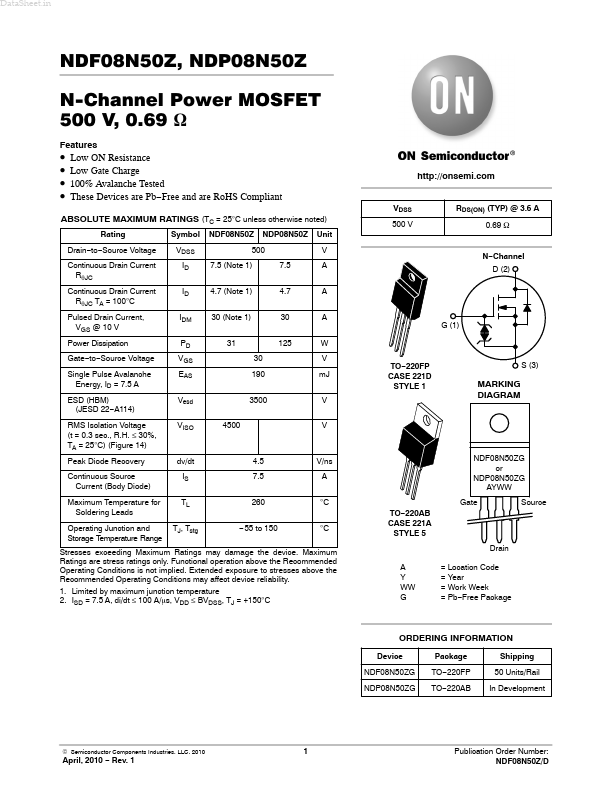
N- Channel D (2)
G (1)
TO- 220FP CASE 221D STYLE 1
S (3)
MARKING DIAGRAM dv/dt IS TL TJ, Tstg
4.5 7.5 260
- 55 to 150
V/ns A °C...