Datasheet Details
| Part number | NCV8161 |
|---|---|
| Manufacturer | ON Semiconductor |
| File Size | 902.68 KB |
| Description | LDO Regulator |
| Datasheet |
 NCV8161 Datasheet NCV8161 Datasheet
|
|
|
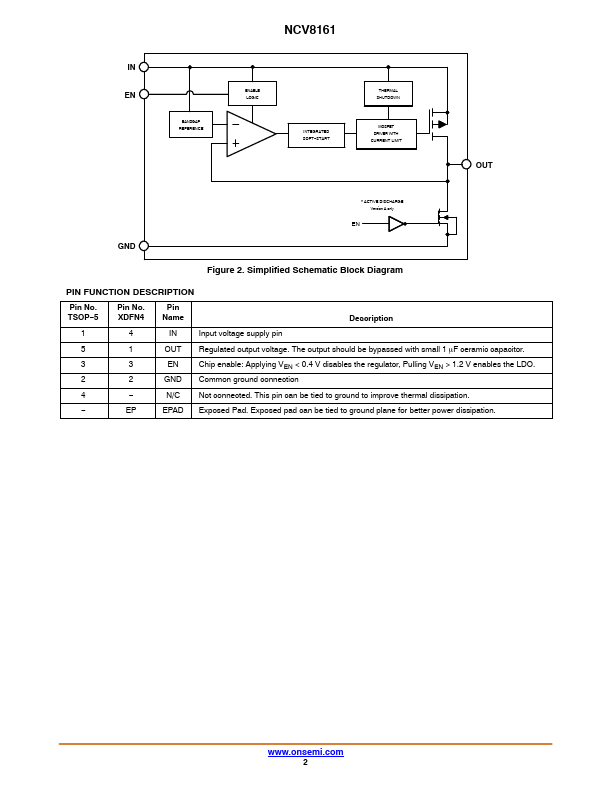
Pin No.
Pin No.
OUT Regulated output voltage.
The output should be bypassed with small 1 mF ceramic capacitor.
| Part number | NCV8161 |
|---|---|
| Manufacturer | ON Semiconductor |
| File Size | 902.68 KB |
| Description | LDO Regulator |
| Datasheet |
NCV8161 Datasheet
|
|
|
|