Datasheet4U Logo Datasheet4U.com

NCV51411 - Low Voltage Buck Regulator

Description

SO-8 SO-16 DFN-18 PIN SYMBOL 1 15 1 BOOST 2 16 2, 3, 4 3 1 5, 6, 7 VIN VSW 4 2 8 SHDNB 5 7 10 6 8 13 7 9 16 SYNC GND VFB 8 10 17 VC - 3 - 6, 9, 11, 12, NC 11 - 14, 15, 18 14 FUNCTION The BOOST pin provides additional drive voltage to the on-chip NPN power transis

Features

  • V2 Architecture Provides Ultra-Fast Transient Response, Improved Regulation and Simplified Design.
  • 2.0% Error Amp Reference Voltage Tolerance.
  • Switch Frequency Decrease of 4:1 in Short Circuit Conditions Reduces Short Circuit Power Dissipation.
  • BOOST Lead Allows “Bootstrapped" Operation to Maximize Efficiency.
  • Sync Function for Parallel Supply Operation or Noise Minimization.
  • Shutdown Pin Provides Power-Down Option.
  • 85 mA Quiescent.

📥 Download Datasheet

Datasheet Details

Part number NCV51411
Manufacturer onsemi
File Size 351.21 KB
Description Low Voltage Buck Regulator
Datasheet download datasheet NCV51411 Datasheet
Other Datasheets by ON Semiconductor

Full PDF Text Transcription

Click to expand full text
DATA SHEET www.onsemi.com 
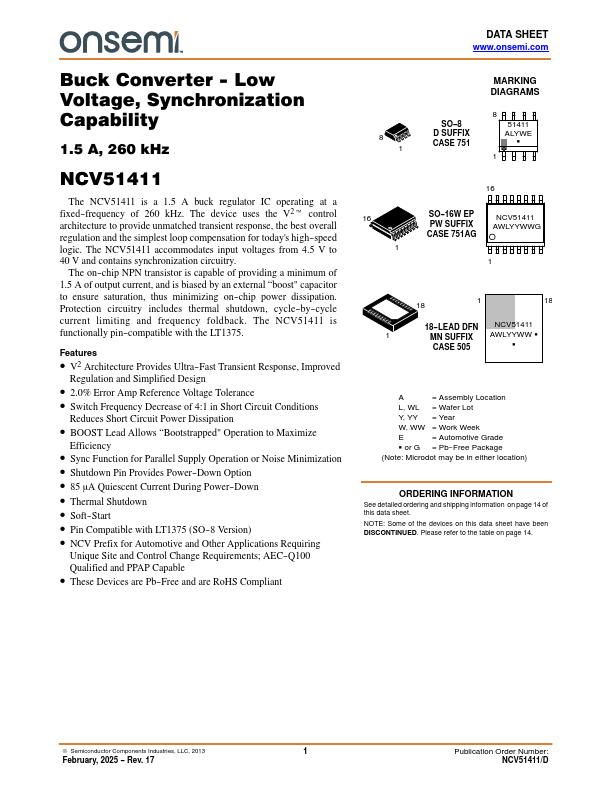
Buck Converter - Low Voltage, Synchronization Capability 1.5 A, 260 kHz NCV51411 
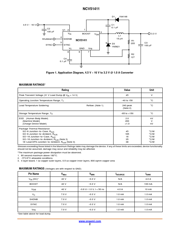
The NCV51411 is a 1.5 A buck regulator IC operating at a fixed-frequency of 260 kHz. The device uses the V2t control architecture to provide unmatched transient response, the best overall regulation and the simplest loop compensation for today's high-speed logic. The NCV51411 accommodates input voltages from 4.5 V to 40 V and contains synchronization circuitry. The on-chip NPN transistor is capable of providing a minimum of 1.5 A of output current, and is biased by an external “boost" capacitor to ensure saturation, thus minimizing on-chip power dissipation. Protection circuitry includes thermal shutdown, cycle-by-cycle current limiting and frequency foldback.
Published: |