Datasheet Details
| Part number | NCP139 |
|---|---|
| Manufacturer | ON Semiconductor |
| File Size | 536.42 KB |
| Description | LDO Regulator |
| Datasheet |
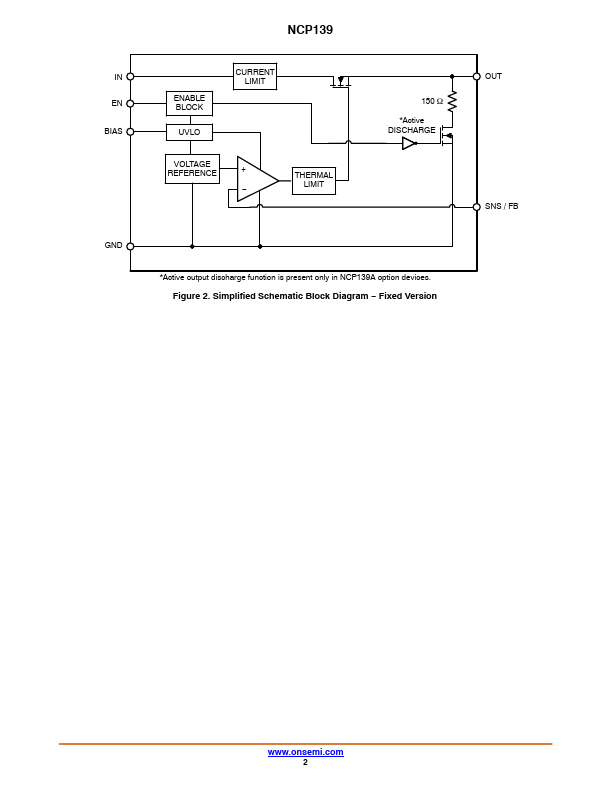
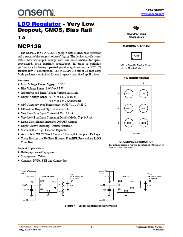
 NCP139 Datasheet NCP139 Datasheet
|
|
|
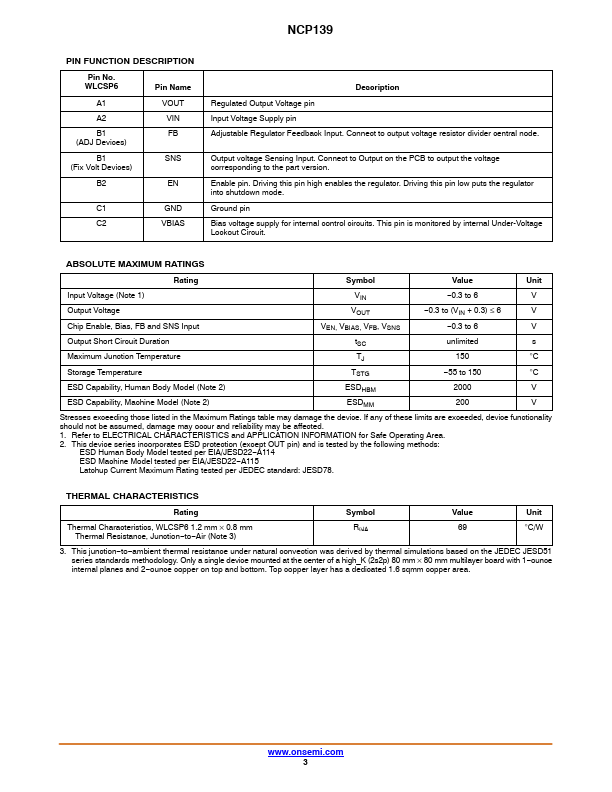
Pin No.
Description Regulated Output Voltage pin Input Voltage Supply pin Adjustable Regulator Feedback Input.
Connect to output voltage resistor divider central node.
| Part number | NCP139 |
|---|---|
| Manufacturer | ON Semiconductor |
| File Size | 536.42 KB |
| Description | LDO Regulator |
| Datasheet |
NCP139 Datasheet
|
|
|
|