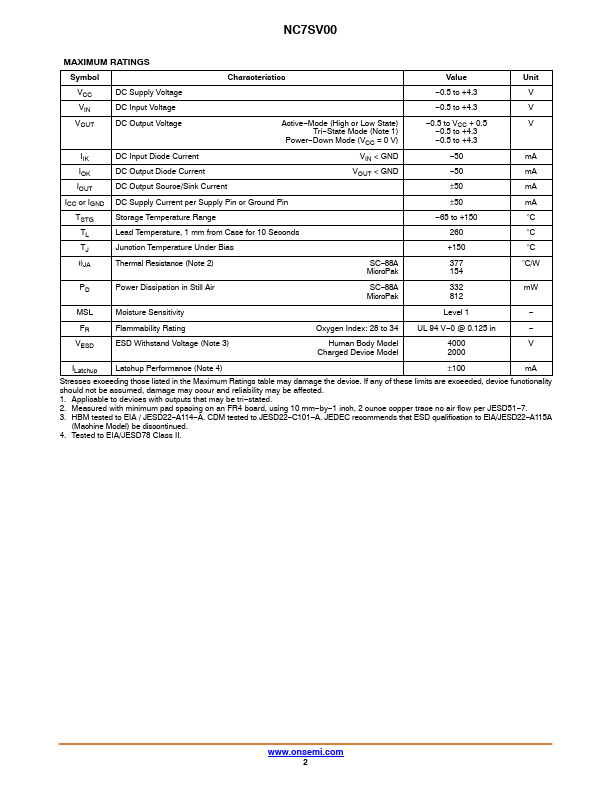
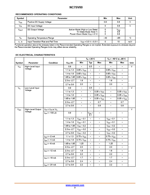
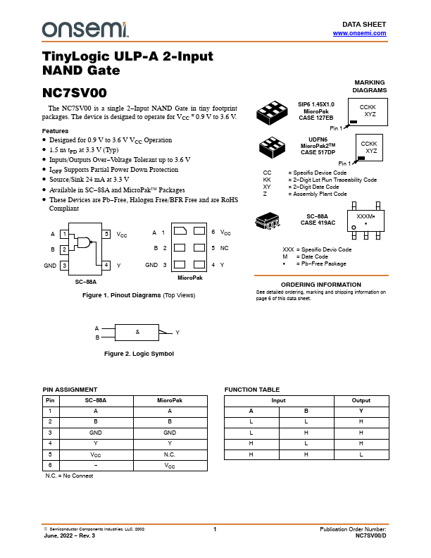
Datasheet4U Logo Datasheet4U.com

NC7SV00 - TinyLogic ULP-A 2-Input NAND Gate

Datasheet Summary

Features

  • Designed for 0.9 V to 3.6 V VCC Operation.
  • 1.5 ns tPD at 3.3 V (Typ).
  • Inputs/Outputs Over.
  • Voltage Tolerant up to 3.6 V.
  • IOFF Supports Partial Power Down Protection.
  • Source/Sink 24 mA at 3.3 V.
  • Available in SC.
  • 88A and MicroPak™ Packages.
  • These Devices are Pb.
  • Free, Halogen Free/BFR Free and are RoHS Compliant A1 B2 5 VCC A1 B2 6 VCC 5 NC GND 3 4Y GND 3 4Y SC.
  • 88A MicroPak Figure 1. Pinout Diag.

📥 Download Datasheet

Datasheet preview – NC7SV00

Datasheet Details

Part number NC7SV00
Manufacturer ON Semiconductor
File Size 347.06 KB
Description TinyLogic ULP-A 2-Input NAND Gate
Datasheet download datasheet NC7SV00 Datasheet
Additional preview pages of the NC7SV00 datasheet.
Other Datasheets by ON Semiconductor

Full PDF Text Transcription

Click to expand full text
TinyLogic ULP-A 2-Input NAND Gate NC7SV00 The NC7SV00 is a single 2−Input NAND Gate in tiny footprint packages. The device is designed to operate for VCC = 0.9 V to 3.6 V. Features • Designed for 0.9 V to 3.6 V VCC Operation • 1.5 ns tPD at 3.3 V (Typ) • Inputs/Outputs Over−Voltage Tolerant up to 3.6 V • IOFF Supports Partial Power Down Protection • Source/Sink 24 mA at 3.3 V • Available in SC−88A and MicroPak™ Packages • These Devices are Pb−Free, Halogen Free/BFR Free and are RoHS Compliant A1 B2 5 VCC A1 B2 6 VCC 5 NC GND 3 4Y GND 3 4Y SC−88A MicroPak Figure 1. Pinout Diagrams (Top Views) DATA SHEET www.onsemi.com MARKING DIAGRAMS SIP6 1.45X1.
Published: |