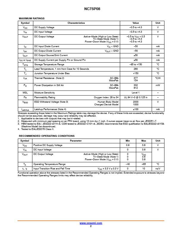
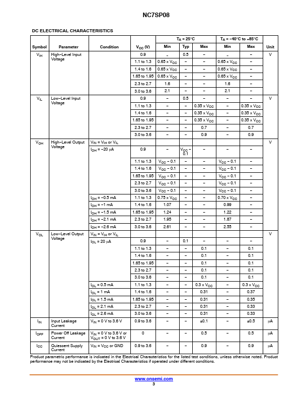
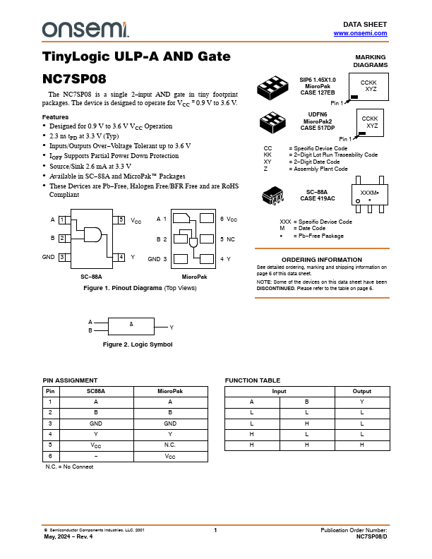
Datasheet4U Logo Datasheet4U.com

NC7SP08 - TinyLogic ULP-A AND Gate

Datasheet Summary

Features

  • Designed for 0.9 V to 3.6 V VCC Operation.
  • 2.3 ns tPD at 3.3 V (Typ).
  • Inputs/Outputs Over.
  • Voltage Tolerant up to 3.6 V.
  • IOFF Supports Partial Power Down Protection.
  • Source/Sink 2.6 mA at 3.3 V.
  • Available in SC.
  • 88A and MicroPak Packages.
  • These Devices are Pb.
  • Free, Halogen Free/BFR Free and are RoHS Compliant A1 B2 GND 3 5 VCC A1 6 VCC B2 5 NC 4 Y GND 3 4Y SC.
  • 88A MicroPak Figure 1. Pinout Diagrams (Top Views) DATA SHE.

📥 Download Datasheet

Datasheet preview – NC7SP08

Datasheet Details

Part number NC7SP08
Manufacturer ON Semiconductor
File Size 350.38 KB
Description TinyLogic ULP-A AND Gate
Datasheet download datasheet NC7SP08 Datasheet
Additional preview pages of the NC7SP08 datasheet.
Other Datasheets by ON Semiconductor

Full PDF Text Transcription

Click to expand full text
TinyLogic ULP-A AND Gate NC7SP08 The NC7SP08 is a single 2−input AND gate in tiny footprint packages. The device is designed to operate for VCC = 0.9 V to 3.6 V. Features  Designed for 0.9 V to 3.6 V VCC Operation  2.3 ns tPD at 3.3 V (Typ)  Inputs/Outputs Over−Voltage Tolerant up to 3.6 V  IOFF Supports Partial Power Down Protection  Source/Sink 2.6 mA at 3.3 V  Available in SC−88A and MicroPak Packages  These Devices are Pb−Free, Halogen Free/BFR Free and are RoHS Compliant A1 B2 GND 3 5 VCC A1 6 VCC B2 5 NC 4 Y GND 3 4Y SC−88A MicroPak Figure 1. Pinout Diagrams (Top Views) DATA SHEET www.onsemi.com MARKING DIAGRAMS SIP6 1.45X1.
Published: |