Datasheet Details
| Part number | NBXSBA019 |
|---|---|
| Manufacturer | onsemi |
| File Size | 156.74 KB |
| Description | Clock Oscillator |
| Datasheet |
 NBXSBA019 Datasheet NBXSBA019 Datasheet
|
|
|
This page provides the datasheet information for the NBXSBA019, a member of the NBXDBA019 Clock Oscillator family.
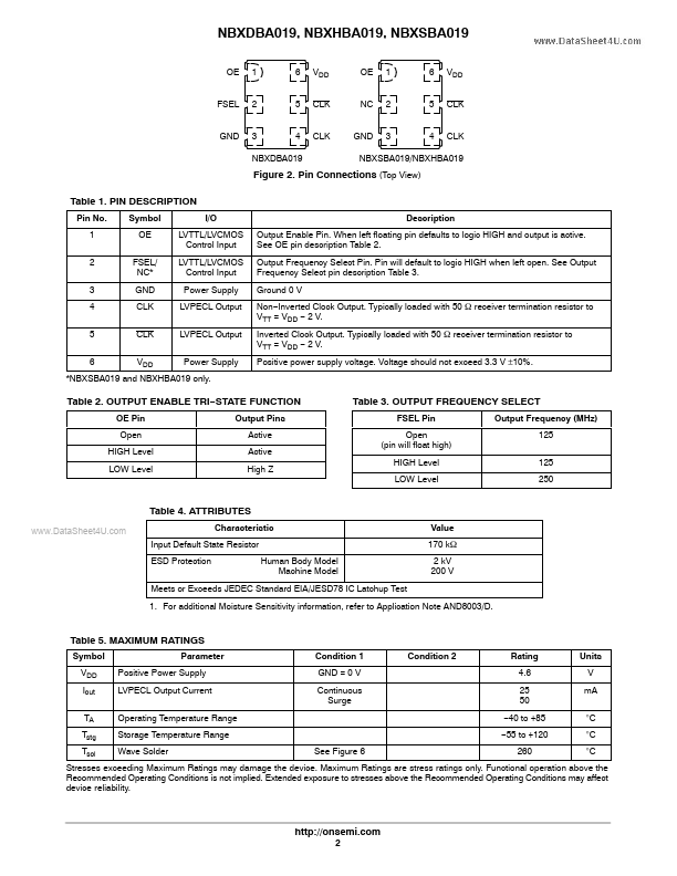
LVTTL/LVCMOS Control Input LVTTL/LVCMOS Control Input Power Supply Output Enable Pin.
When left floating pin defaults to logic HIGH and output is active.
See OE pin description Table 2.
GND CLK CLK VDD Output Frequency Select Pin.
Pin will default to logic HIGH when left open.
| Part number | NBXSBA019 |
|---|---|
| Manufacturer | onsemi |
| File Size | 156.74 KB |
| Description | Clock Oscillator |
| Datasheet |
NBXSBA019 Datasheet
|
|
|
|