MJD128T4G
Features http://onsemi.
ÎÎÎÎÎÎÎÎÎÎÎÎÎÎÎÎÎÎÎ ÎÎÎÎÎÎÎÎÎÎÎÎÎÎÎÎÎÎÎ
MAXIMUM RATINGS
Rating Symbol VCEO VCB VEB Continuous Peak IC IB PD PD TJ, Tstg Value 120 120 5 8 16 120 20 0.16 1.75 0.014
- 65 to + 150 Unit Vdc Vdc Vdc Adc m Adc W W/°C W W/°C °C Collector- Emitter Voltage Collector- Base Voltage Emitter- Base Voltage Collector Current
- Base Current Total Power Dissipation @ TC = 25°C Derate above 25°C Total Power Dissipation- @ TA = 25°C Derate above 25°C Operating and Storage Junction Temperature Range
Designed for general purpose amplifier and low speed switching applications.
- Monolithic Construction With Built- in Base- Emitter Shunt Resistors
- High DC Current Gain
- h FE = 2500 (Typ) @ IC = 4.0 Adc
- Epoxy Meets UL 94 V- 0 @ 0.125 in.
- ESD Ratings: Human Body Model, 3B u 8000 V Machine Model, C u 400 V
- This is a Pb- Free Device
SILICON POWER TRANSISTOR 8 AMPERES 120 VOLTS, 20 WATTS
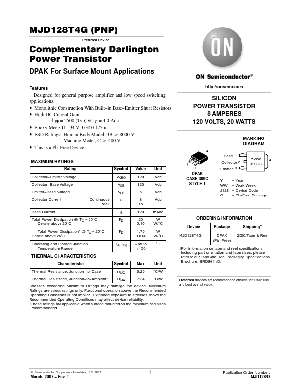
MARKING DIAGRAM
4 Base 1 1 2 3 DPAK CASE 369C STYLE 1 Collector 2 Emitter 3 Y WW J128 G = Year =...