Download the MC74AC240 datasheet PDF.
This datasheet also covers the MC74ACT240 variant, as both devices belong to the same octal buffer/line driver family and are provided as variant models within a single manufacturer datasheet.
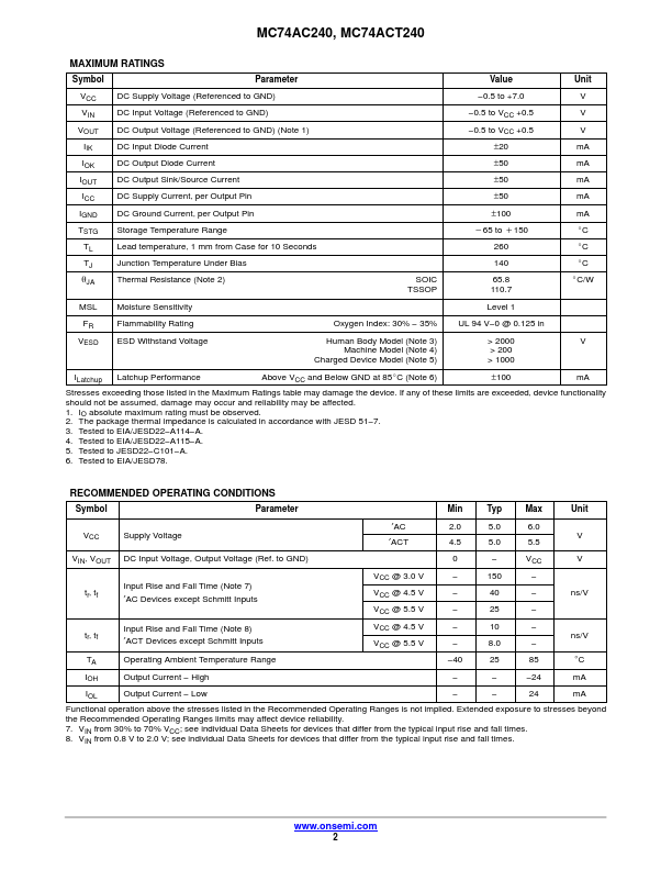
Key Features
3.
State Outputs Drive Bus Lines or Buffer Memory Address
Registers.
Outputs Source/Sink 24 mA.
′ACT240 Has TTL Compatible Inputs.
These are Pb.
Free Devices
TRUTH TABLE
Inputs
Outputs
OE1 D (Pins 12, 14, 16, 18)
LL LH HX
H L Z
NOTE:
H = HIGH Voltage Level L = LOW Voltage Level X = Immaterial Z = High Impedance
TRUTH TABLE
Inputs
Outputs
OE2 D
LL LH HX
(Pins 3, 5, 7, 9)
H L Z
NOTE:
H = HIGH Voltage Level L = LOW Voltage Level X =.
Full PDF Text Transcription for MC74AC240 (Reference)
Note: Below is a high-fidelity text extraction (approx. 800 characters) for
MC74AC240. For precise diagrams, and layout, please refer to the original PDF.
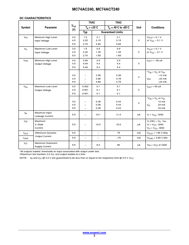
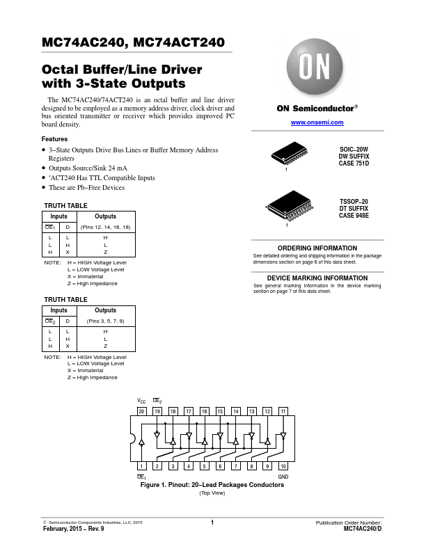
MC74AC240, MC74ACT240 Octal Buffer/Line Driver with 3-State Outputs The MC74AC240/74ACT240 is an octal buffer and line driver designed to be employed as a memory address ...
View more extracted text
al buffer and line driver designed to be employed as a memory address driver, clock driver and bus oriented transmitter or receiver which provides improved PC board density. Features • 3−State Outputs Drive Bus Lines or Buffer Memory Address Registers • Outputs Source/Sink 24 mA • ′ACT240 Has TTL Compatible Inputs • These are Pb−Free Devices TRUTH TABLE Inputs Outputs OE1 D (Pins 12, 14, 16, 18) LL LH HX H L Z NOTE: H = HIGH Voltage Level L = LOW Voltage Level X = Immaterial Z = High Impedance TRUTH TABLE Inputs Outputs OE2 D LL LH HX (Pins 3, 5, 7, 9) H L Z NOTE: H = HIGH Voltage Level L = LOW Voltage Level X = Immaterial
 MC74AC240 Datasheet