Datasheet Details
| Part number | MC74AC174 |
|---|---|
| Manufacturer | onsemi |
| File Size | 251.71 KB |
| Description | Hex D Flip-Flop |
| Datasheet |
 MC74AC174 Datasheet MC74AC174 Datasheet
|
|
|
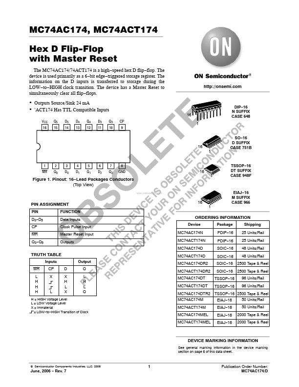
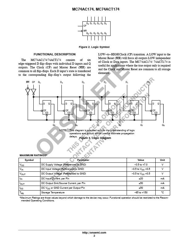
flops with individual D inputs and Q outputs.
flops.
flop’s output following the MR C| Part number | MC74AC174 |
|---|---|
| Manufacturer | onsemi |
| File Size | 251.71 KB |
| Description | Hex D Flip-Flop |
| Datasheet |
MC74AC174 Datasheet
|
|
|
|
Note: Below is a high-fidelity text extraction (approx. 800 characters) for MC74AC174. For precise diagrams, and layout, please refer to the original PDF.
MC74AC174, MC74ACT174 Hex D Flip−Flop with Master Reset The MC74AC174/74ACT174 is a high−speed hex D flip−flop. The device is used primarily as a 6−bit edge−triggered sto...
| Part Number | Description |
|---|---|
| MC74AC175 | Quad D Flip-Flop |
| MC74AC10 | Triple 3-Input NAND Gate |
| MC74AC109 | Dual JK Positive Edge Triggered Flip-Flop |
| MC74AC11 | Triple 3-Input AND Gate |
| MC74AC125 | Quad Buffer |
| MC74AC132 | Quad 2-Input NAND Schmitt Trigger |
| MC74AC138 | 1-of-8 Decoder / Demultiplexer |
| MC74AC139 | Dual 1-of-4 Decoder/Demultiplexer |
| MC74AC14 | Hex Inverter Schmitt Trigger |
| MC74AC151 | 1-of-8 Decoder / Demultiplexer |