Protection diode in
Specifications
Absolute Maximum Ratings at Ta=25°C
Parameter
Symbol
Drain-to-Source Voltage Gate-to-Source Voltage Drain Current (DC) Drain Current (PW≤100ms)
VDSS VGSS ID IDP
Drain Current (PW≤10μs) Allowable Power Dissipatio.
Note: Below is a high-fidelity text extraction (approx. 800 characters) for
FW389. For precise diagrams, and layout, please refer to the original PDF.
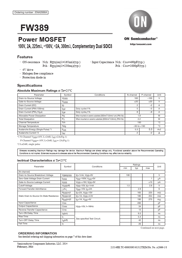
Ordering number : ENA2066A FW389 Power MOSFET 100V, 2A, 225mΩ, –100V, –2A, 300mΩ, Complementary Dual SOIC8 http://onsemi.com Features • ON-resistance Nch : RDS(on)1=165mW...
View more extracted text
SOIC8 http://onsemi.com Features • ON-resistance Nch : RDS(on)1=165mW(typ.) • Input Capacitance Nch : Ciss=490pF(typ.) Pch : RDS(on)1=230mW(typ.) Pch : Ciss=1000pF(typ.) • 4V drive • Halogen free compliance • Protection diode in Specifications Absolute Maximum Ratings at Ta=25°C Parameter Symbol Drain-to-Source Voltage Gate-to-Source Voltage Drain Current (DC) Drain Current (PW≤100ms) VDSS VGSS ID IDP Drain Current (PW≤10μs) Allowable Power Dissipation Total Dissipation Channel Temperature IDP PD PT Tch Storage Temperature Tstg Avalanche Energy (Single Pulse) *1 Avalanche Current *2 EAS IAV *1 N-Channel:VDD=10V, L=2mH, IA
 FW389 Datasheet