FDS6673BZ-F085
Description
Features
- Max r DS(on) = 7.8mΩ, VGS = -10V, ID = -14.5A
This P-Channel MOSFET is produced using ON Semiconductor’s advanced Power Trench process that has been especially tailored to minimize the on-state
- Max r DS(on) = 12mΩ, VGS = -4.5V, ID = -12A
- Extended VGS range (-25V) for battery applications resistance.
- HBM ESD protection level of 6.5k V typical (note 3)
This device is well suited for Power Management and load switching applications mon in Notebook puters and Portable Battery Packs.
- High performance trench technology for extremely low r DS(on)
- High power and current handling capability
- Ro HS pliant
- Qualified to AEC Q101
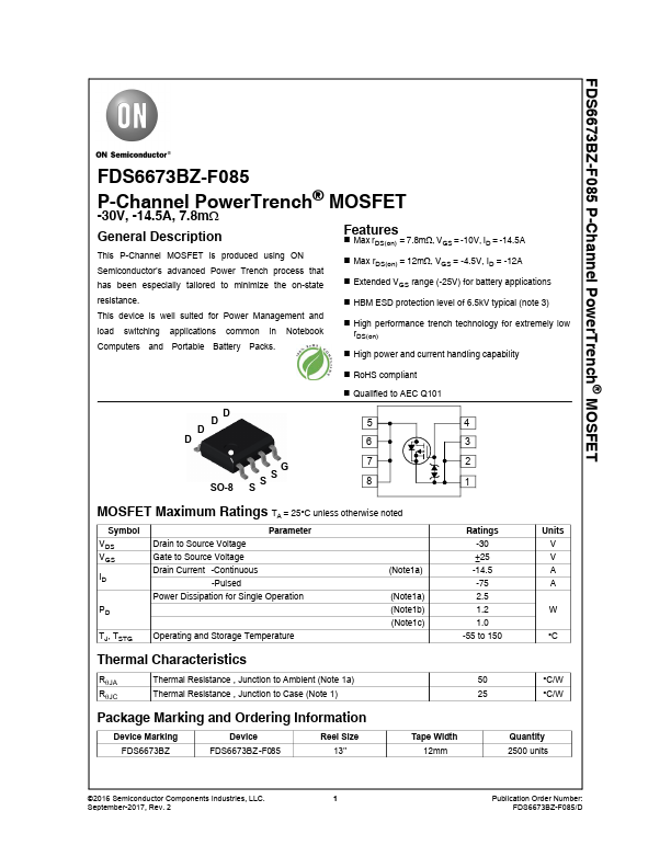
SO-8
SS S
MOSFET Maximum Ratings TA = 25°C unless otherwise noted
Symbol VDS VGS
Drain to Source Voltage Gate to Source Voltage Drain Current -Continuous
-Pulsed
Parameter
(Note1a)
Power Dissipation for Single Operation
(Note1a)
PD TJ, TSTG
Operating and Storage Temperature
(Note1b)...