Datasheet Details
| Part number | FDMC610P |
|---|---|
| Manufacturer | ON Semiconductor |
| File Size | 369.32 KB |
| Description | P-Channel MOSFET |
| Datasheet |
 FDMC610P Datasheet FDMC610P Datasheet
|
|
|
| Part number | FDMC610P |
|---|---|
| Manufacturer | ON Semiconductor |
| File Size | 369.32 KB |
| Description | P-Channel MOSFET |
| Datasheet |
FDMC610P Datasheet
|
|
|
|
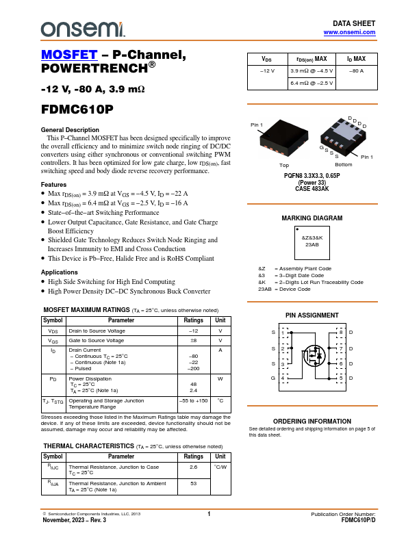
This P Channel MOSFET has been designed specifically to improve the overall efficiency and to minimize switch node ringing of DC/DC converters using either synchronous or conventional switching PWM controllers.It has been optimized for low gate charge, low rDS(on), fast switching speed and body diode reverse recovery performance.
📁 Similar Datasheet