Click to expand full text
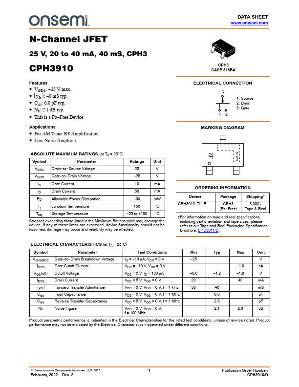
DATA SHEET www.onsemi.com
N-Channel JFET
25 V, 20 to 40 mA, 40 mS, CPH3
CPH3910
Features
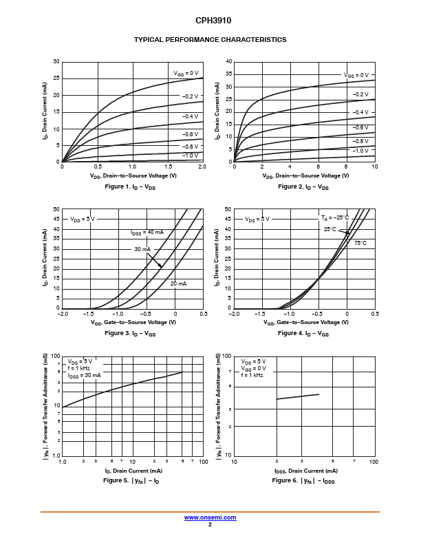
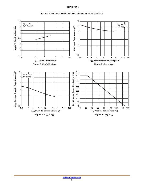
• VGDS: −25 V max. • ⎢yfs⎥ : 40 mS typ. • Ciss: 6.0 pF typ. • NF: 2.1 dB typ. • This is a Pb−Free Device
Applications
• For AM Tuner RF Amplification • Low Noise Amplifier
ABSOLUTE MAXIMUM RATINGS (at TA = 25°C)
Symbol
Parameter
Ratings Unit
VDSX Drain−to−Source Voltage
25
V
VGDS Gate−to−Drain Voltage
−25
V
IG
Gate Current
10
mA
ID
Drain Current
50
mA
PD
Allowable Power Dissipation
400
mW
Tj
Junction Temperature
150
°C
Tstg Storage Temperature
−55 to +150 °C
Stresses exceeding those listed in the Maximum Ratings table may damage the device. If any of these limits are exceeded, device functionality should not be assumed, damage may occur and reliability may be affected.
 CPH3910 Datasheet