Click to expand full text
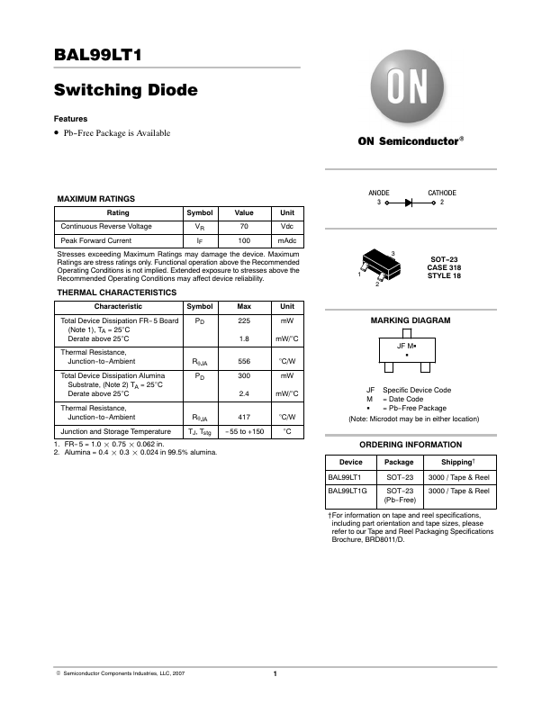
BAL99LT1
Switching Diode
Features
•ăPb-Free Package is Available
MAXIMUM RATINGS
Rating
Symbol
Value
Unit
Continuous Reverse Voltage
VR 70 Vdc
Peak Forward Current
IF 100 mAdc
Stresses exceeding Maximum Ratings may damage the device. Maximum Ratings are stress ratings only. Functional operation above the Recommended Operating Conditions is not implied. Extended exposure to stresses above the Recommended Operating Conditions may affect device reliability.
THERMAL CHARACTERISTICS
Characteristic
Symbol
Max
Unit
Total Device Dissipation FR-ā5 Board
(Note 1), TA = 25°C Derate above 25°C
PD
225 mW 1.8 mW/°C
Thermal Resistance, Junction-to-Ambient
Total Device Dissipation Alumina Substrate, (Note 2) TA = 25°C Derate above 25°C
RqJA PD
556 °C/W 300 mW 2.
 BAL99LT1 Datasheet