Datasheet4U Logo Datasheet4U.com

74FST3253 - Dual 4:1 Multiplexer/Demultiplexer Bus Switch

Description

See detailed ordering and shipping information in the package dimensions section on page 2 of this data sheet.

For additional information on our Pb Free strategy and soldering details, please download the ON Semiconduct

Features

  • RON t 4 W Typical.
  • Less Than 0.25 ns.
  • Max Delay Through Switch.
  • Nearly Zero Standby Current.
  • No Circuit Bounce.
  • Control Inputs are TTL/CMOS Compatible.
  • Pin.
  • For.
  • Pin Compatible With QS3253, FST3253, CBT3253.
  • Popular Packages: TSSOP.
  • 16, SOIC.
  • 16.
  • All Devices in Package TSSOP are Inherently Pb.
  • Free.
  • OE1 S1 1B4 1B3 1B2 1B1 1A GND 1 2 3 4 5 6 7 8 16 VCC 15 OE2 14 S0 13 2B4.

📥 Download Datasheet

Datasheet Details

Part number 74FST3253
Manufacturer onsemi
File Size 182.72 KB
Description Dual 4:1 Multiplexer/Demultiplexer Bus Switch
Datasheet download datasheet 74FST3253 Datasheet

Full PDF Text Transcription

Click to expand full text
74FST3253 
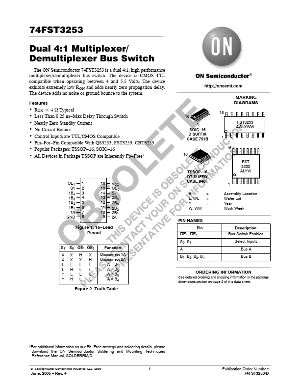
Dual 4:1 Multiplexer/ Demultiplexer Bus Switch 
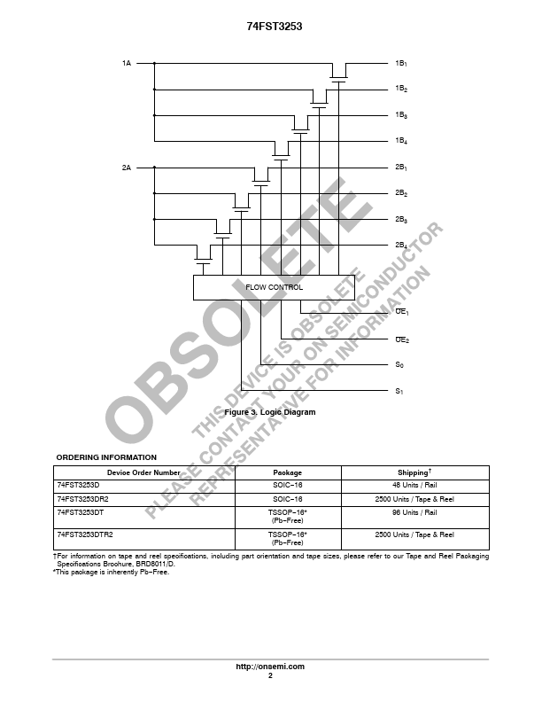
The ON Semiconductor 74FST3253 is a dual 4:1, high performance multiplexer/demultiplexer bus switch. The device is CMOS TTL compatible when operating between 4 and 5.5 Volts. The device exhibits extremely low RON and adds nearly zero propagation delay. The device adds no noise or ground bounce to the system. Features • RON t 4 W Typical • Less Than 0.25 ns−Max Delay Through Switch • Nearly Zero Standby Current • No Circuit Bounce • Control Inputs are TTL/CMOS Compatible • Pin−For−Pin Compatible With QS3253, FST3253, CBT3253 • Popular Packages: TSSOP−16, SOIC−16 • All Devices in Package TSSOP are Inherently Pb−Free* OE1 S1 1B4 1B3 1B2 1B1 1A GND 1 2 3 4 5 6 7 8 16 VCC 15 OE2 14 S0 13 2B4 12 11 10 9 2B3 2B2 2B1 2A Figure 1.
Published: |