2SC5226A
Features
- Low- noise: NF = 1.0 d B Typ (f = 1 GHz)
- High Gain: ⎪S21e⎪2 = 12 d B Typ (f = 1 GHz)
- High Cut- off Frequency: f T = 7 GHz Typ
- This is a Pb- Free Device
Specifications
ABSOLUTE MAXIMUM RATINGS (TA = 25°C)
Symbol
Parameter
Value
Unit
VCBO VCEO VEBO
IC PC Tj
Collector- to- Base Voltage Collector- to- Emitter Voltage Emitter- to- Base Voltage Collector Current Collector Dissipation Junction Temperature
70 m A
150 m W
°C
Tstg Storage Temperature
- 55 to +150 °C
Stresses exceeding those listed in the Maximum Ratings table may damage the device. If any of these limits are exceeded, device functionality should not be assumed, damage may occur and reliability may be affected.
DATA SHEET .onsemi.
1 2
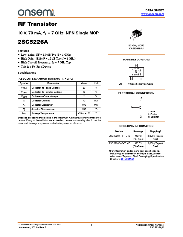
SC- 70 / MCP3 CASE 419AJ
MARKING DIAGRAM
LOT No.
LN R A N K LOT No.
= Specific Device Code
ELECTRICAL CONNECTION 3
1: Base
2: Emitter
3: Collector
ORDERING INFORMATION
Device
Package...