Click to expand full text
NJW4190
Doubler Charge Pump IC
GENERAL DESCRIPTION
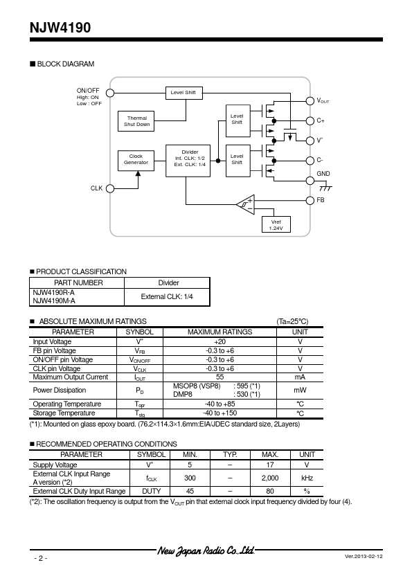
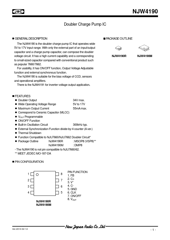
The NJW4190 is the doubler charge pump IC that operates wide 5V to 17V input range. With only the external part of an input/output capacitor and a charge pump capacitor, can compose the doubler voltage circuit. It has a high current capability and a corresponding to small-sized capacitor compared with conventional product such as popular 7660/7662. For usability, it has ON/OFF function, Output Voltage Adjustable function and external synchronous function. The NJW4190 is suitable for the bias voltage of CCD, sensors and operational amplifiers. There is the NJW4191 for inverter voltage output application.
PACKAGE OUTLINE
NJW4190R
NJW4190M
FEATURES Doubler Output 34V max.
 NJW4190 Datasheet