Datasheet Details
| Part number | DS90LV028A |
|---|---|
| Manufacturer | National Semiconductor (now Texas Instruments) |
| File Size | 247.02 KB |
| Description | 3V LVDS Dual CMOS Differential Line Receiver |
| Datasheet |
 DS90LV028A Datasheet DS90LV028A Datasheet
|
|
|
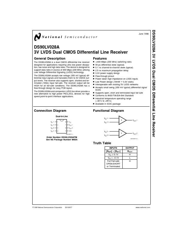
The DS90LV028A is a dual CMOS differential line receiver designed for applications requiring ultra low power dissipation, low noise and high data rates.
The device is designed to support data rates in excess of 400 Mbps (200 MHz) utilizing Low Voltage Differential Signaling (LVDS) technology.
| Part number | DS90LV028A |
|---|---|
| Manufacturer | National Semiconductor (now Texas Instruments) |
| File Size | 247.02 KB |
| Description | 3V LVDS Dual CMOS Differential Line Receiver |
| Datasheet |
DS90LV028A Datasheet
|
|
|
|
| Part Number | Description | Manufacturer |
|---|---|---|
| DS90LV028A | 3-V LVDS Dual CMOS Differential Line Receiver | Texas Instruments |
| DS90LV028AH | high temperature 3-V LVDS dual differential line receiver | Texas Instruments |
| DS90LV028AQ | Automotive LVDS Dual Differential Line Receiver | Texas Instruments |
| DS90LV028AQ-Q1 | Automotive LVDS Dual Differential Line Receiver | Texas Instruments |
| Part Number | Description |
|---|---|
| DS90LV028AH | High Temperature 3V LVDS Dual Differential Line Receiver |
| DS90LV028AQ | Automotive LVDS Dual Differential Line Receiver |
| DS90LV027 | LVDS Dual High Speed Differential Driver |
| DS90LV027A | LVDS Dual High Speed Differential Driver |
| DS90LV001 | 3.3V LVDS-LVDS Buffer |
| DS90LV004 | 4-Channel LVDS Buffer/Repeater |
| DS90LV011A | 3V LVDS Single High Speed Differential Driver |
| DS90LV012A | 3V LVDS Single CMOS Differential Line Receiver |
| DS90LV017 | LVDS Single High Speed Differential Driver |
| DS90LV017A | LVDS Single High Speed Differential Driver |
The following content is an automatically extracted verbatim text from the original manufacturer datasheet and is provided for reference purposes only.