Datasheet4U Logo Datasheet4U.com

CGS74B2529 - 1 to 10 Minimum Skew Clock Driver

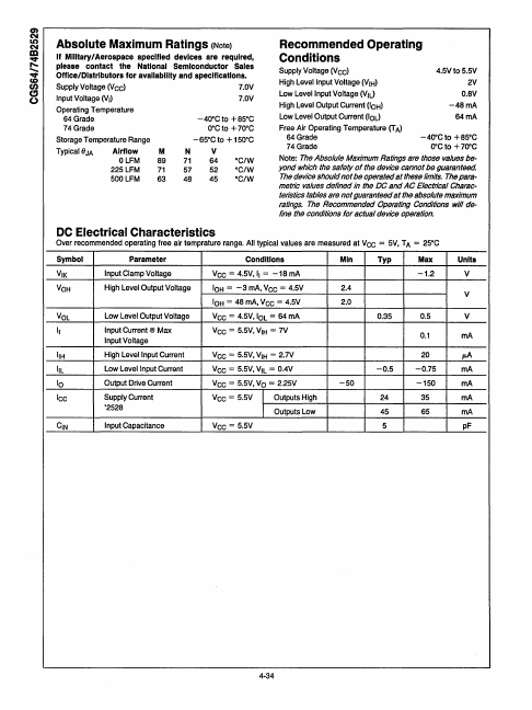
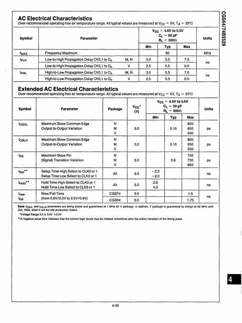
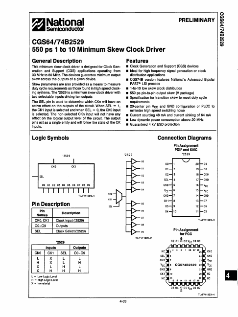
This page provides the datasheet information for the CGS74B2529, a member of the CGS6482529 1 to 10 Minimum Skew Clock Driver family.

Description

This minimum skew clock driver is designed for Clock Gen

eration and Support (CGS) applications operating from 33 MHz to 80 MHz.

The devices guarantee minimum output skew across the outputs of a given device.

Features

  • Clock Generation and Support (CGS) devices.
  • Ideal for high frequency signal generation or clock distribution.

📥 Download Datasheet

Datasheet preview – CGS74B2529

Datasheet Details

Part number CGS74B2529
Manufacturer National Semiconductor
File Size 122.12 KB
Description 1 to 10 Minimum Skew Clock Driver
Datasheet download datasheet CGS74B2529 Datasheet
Additional preview pages of the CGS74B2529 datasheet.
Other Datasheets by National Semiconductor

Full PDF Text Transcription

Click to expand full text
~~ NaStemiicoonnduactlor PRELIMINARY CGS64/7482529 550 ps 1 to 10 Minimum Skew Clock Driver General Description This minimum skew clock driver is designed for Clock Gen· eration and Support (CGS) applications operating from 33 MHz to 80 MHz. The devices guarantee minimum output skew across the outputs of a given device. Skew parameters are also provided as a means to measure duty cycle requirements as those found in high speed clock· ing systems. The '2529 is a minimum skew clock driver with two selectable inputs driving ten outputs The SEL pin is used to determine which CKn will have an active effect on the outputs of the circuit. When SEL = 1, the CK1 input is selected and when SEL = 0, the CKO input is selected.
Published: |