The following content is an automatically extracted verbatim text
from the original manufacturer datasheet and is provided for reference purposes only.
View original datasheet text
PDF: 2003 Apr 07
Philips Semiconductors
Package outline
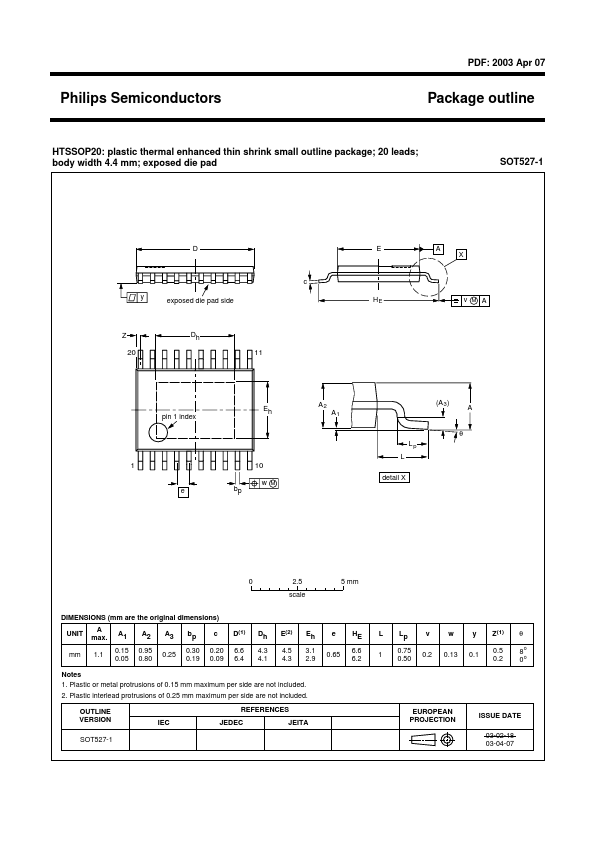
HTSSOP20: plastic thermal enhanced thin shrink small outline package; 20 leads; body width 4.4 mm; exposed die pad
SOT527-1
D
E
A
X
c y exposed die pad side HE v M A
Z
Dh
20
11
pin 1 index
Eh
A2 A1
(A 3)
A θ
Lp L
1
e bp
10
w M detail X
0
2.5 scale
5 mm
DIMENSIONS (mm are the original dimensions) UNIT mm A max. 1.1 A1 0.15 0.05 A2 0.95 0.80 A3 0.25 bp 0.30 0.19 c 0.20 0.09 D(1) 6.6 6.4 Dh 4.3 4.1 E(2) 4.5 4.3 Eh 3.1 2.9 e 0.65 HE 6.6 6.2 L 1 Lp 0.75 0.50 v 0.2 w 0.13 y 0.1 Z(1) 0.5 0.2 θ 8 0o
o
Notes 1. Plastic or metal protrusions of 0.15 mm maximum per side are not included. 2. Plastic interlead protrusions of 0.25 mm maximum per side are not included.
 SOT527-1 Datasheet